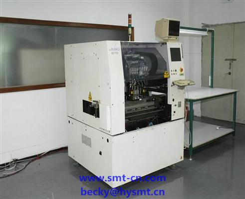
Juki SMT process flow
Model: |
Juki SMT process flow |
Category: |
|
Condition: |
|
Location: |
China |
Offered by: |
|
|
SMT basic process components include: silk screen (or dispensing), placement (curing), reflow soldering, cleaning, testing, repair
1, silk screen: its role is to paste or patch solder paste printed on the PCB pad, the components for the welding to prepare. The equipment used is silk screen (screen printing machine), located in the front of the SMT production line.
2, dispensing: it is the glue drops to the fixed position of the PCB, its main role is to fixed components to the PCB board. The equipment used is a dispenser, located at the front of the SMT production line or behind the testing equipment.
3, the placement: its role is to surface assembly components installed accurately to the fixed location of the PCB. The equipment used is a placement machine, located in the SMT production line behind the silk screen machine.
4, curing: its role is to melt the paste, so that the surface assembly components and PCB board firmly bonded together. The equipment used is a curing furnace, located in the SMT production line in the back of the placement machine.
5, reflow soldering: its role is to melt the paste, so that the surface assembly components and PCB board firmly bonded together. The equipment used is a reflow oven located behind the Mounter in the SMT production line.
6, cleaning: its role is to assemble the PCB board above the human body harmful welding residues such as flux to remove. The equipment used for the cleaning machine, the location can not be fixed, can be online or not online.
7, detection: its role is to assemble the PCB board for welding quality and assembly quality testing. The equipment used is magnifying glass, microscope, online tester (ICT), flying probe tester, automatic optical detection (AOI), X-RAY detection system, function tester. The position can be arranged in the appropriate place of production line according to the need of detection.
8, rework: its role is to detect the failure of the PCB board rework. The tools used are soldering iron, rework station and so on. Configured anywhere in the production line.
First, single-sided assembly:
Material inspection => silk screen solder paste (point patch glue) => patch => drying (curing) => reflow welding => cleaning => detection => repair
Second, double-sided assembly:
A: incoming inspection => PCB A surface silk screen solder paste (point patch glue) => patch => drying (curing) => A surface reflow soldering => cleaning => flap => PCB B side Silk screen solder paste (point patch glue) => patch => drying => reflow soldering (preferably only on the B side => cleaning => detection => repair)
This process is suitable for both sides of the PCB are mounted with PLCC and other large SMD used.
B: incoming inspection => PCB A surface silk screen solder paste (point patch glue) => patch => drying (curing) => A surface reflow soldering => cleaning => flap => PCB B side Point patch glue => patch => curing => B surface wave soldering => cleaning => detection => repair)
This process is suitable for reflow soldering on the A side of the PCB. This process should be used in SMDs assembled on the B side of PCBs only when SOT or SOIC (28) pins are present.
Third, single-sided mixed process:
Supply> Supply> Supply PCB> Supply PCB Supply PCB Supply PCB Supply PCB Supply PCB Supply PCB Supply PCB Supply PCB Supply PCB Supply PCB Supply PCB Supply PCB Information Name: Supply PCB Information Name: Supply PCB Information Name: Supply PCB Published: 2012-03-16 Validity: 30 Specifications: Quantity: 0.00 Price Description: Negotiable Detailed Product Description: > Rework
Four, two-sided mixed process:
A: incoming inspection => PCB B face point patch glue => patch => curing => flap => PCB A side plug => wave soldering => cleaning => detection => repair
The first post-paste, apply to the SMD components more than the separation of the case
B: incoming inspection => PCB A-side plug (pin bend) => flap => PCB B face patch => patch => cure => flap => wave soldering => cleaning => Detection => rework
First post-paste, apply to the separation of components more than SMD components of the situation
C: incoming inspection => PCB A surface silk screen solder paste => patch => drying => reflow soldering => plug, pin bend => flap => PCB B face patch adhesive => Patch => Cure => Flap => Wave Soldering => Cleaning => Test => Rework A-side mix, B-mount.
D: incoming inspection => PCB B surface point patch glue => patch => curing => flap => PCB A side silk screen solder paste => patch => A surface reflow soldering => plugin = B surface wave soldering => cleaning => detection => repair A surface mixed, B surface mount. (Patching) => Patch => Drying (curing) => Reflow soldering = (Can be used for local welding) => plug-in => wave soldering 2 (if the cartridge components are small, you can use manual welding) => Cleaning => test => repair A face mount, B side mixed.
Five, double-sided assembly process
A: incoming inspection, PCB A surface silk screen solder paste (point patch glue), patch, drying (curing), A surface reflow soldering, cleaning, flap; PCB B surface silk screen solder paste (point patch Glue), patch, drying, reflow soldering (preferably only on the B side, cleaning, testing, repair)
This process is suitable for both sides of the PCB are mounted with PLCC and other large SMD used.
B: incoming inspection, PCB A side silk screen printing paste (point patch glue), patch, drying (curing), A surface reflow soldering, cleaning, flap; PCB B surface patch, patch , Curing, B surface wave soldering, cleaning, testing, repair) This process is suitable for the A side of the PCB reflow, B surface wave soldering. This process should be used in SMDs assembled on the B side of PCBs only when SOT or SOIC (28) pins are present.
Becky Su
becky@hysmt.cn
ZK Electronic /Blue Fish
Skype:beckysmt
Wechat / WhatsApp::8615323874439


