Jan 11, 2010
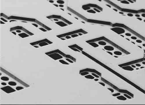
The latest VectorGuard release from DEK is a double-layer stencil fabricated through a two-step lithography and Nickel electroforming process, before being mounted on VectorGuard tensioning technology. Benefiting from DEK’s specialist CAD expertise, the mesh layer of the two-layer structure serves to hold the stencil intact while accurately controlling the flow of paste to the second layer. The circuit layer determines the thickness and shape of the print deposits to deliver high tolerance, fine dimension printing. Ideal for accuracy-critical applications such as solar cell manufacture or LTCC manufacture, the double-layer stencil incorporates the advantages of VectorGuard stencil technology to create a screen alternative that generates a tenfold increase in product lifetime.
VectorGuard Double Layer Platinum stencils feature a wide range of advantages over conventional screen technologies, including the ability to print long conductive lines without diminishing stencil strength. In addition, the system incorporates numerous advantages for microelectronics packaging specialists. Ideal for multi-layer technologies such as Low Temperature Co-fired Ceramic (LTCC), the new VectorGuard technology reduces this two-step process down to just one by combining filling and inner-layer printing stages. Substantially easier to clean and maintain than a screen, the double layer stencils harness the potential of VectorGuard tensioning to generate dimensional accuracy better than 0.1µm/mm. The new DEK stencil also incorporates all the operational advantages of the reusable, recyclable VectorGuard system, including ease-of-use, system rigidity and operator safety. The system also delivers numerous space-saving storage advantages and is complemented by the VectorGuard Cabinet and VectorGuard Workstation.
“Our patented VectorGuard system has long delivered significant advantages over conventional stencil technologies. But now, the unique system also offers a valuable alternative to precision screen technologies, too – as well as combining major advantages for semiconductor packaging and component manufacturing,” explains DEK Product Manager for Stencils, Michael Zahn. “In addition to VectorGuard’s unprecedented process flexibility and yield enhancement, our new double layer Platinum stencils leverage the power of the system to transform the face of screen technologies for manufacturers requiring high accuracy performance. Plus, having dramatically extended product lifetime in relation to traditional screens, this is an extremely cost-efficient solution. We’re very excited about this breakthrough and its ability to give DEK customers around the world another reason to expect more.”
About DEK
DEK is a global provider of advanced materials deposition technologies and support solutions including printing equipment platforms, stencils, precision screens and mass imaging processes used across a wide range of applications in electronics pre-placement subassembly, semiconductor wafer manufacture, and alternative energy component production. For more information, visit DEK at http://www.dek.com.