5G communication board PCB design case
Company Information:
Category: |
|
Offered by: |
|
5G communication board PCB design case Description:
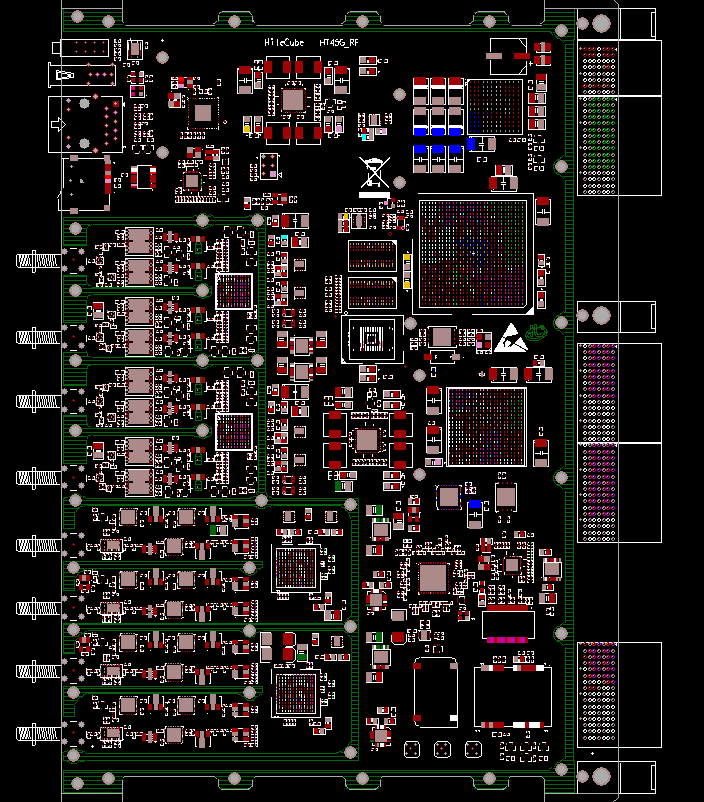
[Single board type] 5G RF communication board (VPX architecture)
[Pin number] 10731
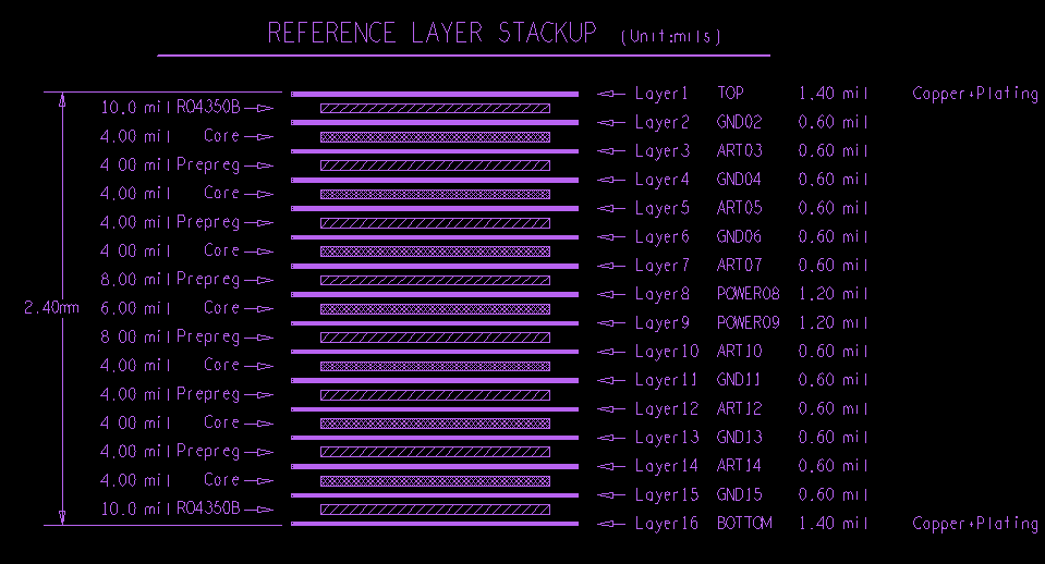
[layers] 16 layers
[Maximum rate] 10Gb/s
[Difficulties]:
1, There are 8 RF channels, the RF line rate is 2.5G, and the requirement of the signal integrity is high;
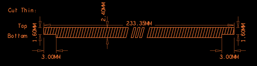
2, The plate thickness is 1.6mm, and the number of laminates is limited;
3, The RF part is more, need to do heat dissipation and shielding;
[Our countermeasures]:
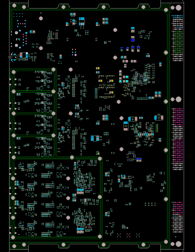
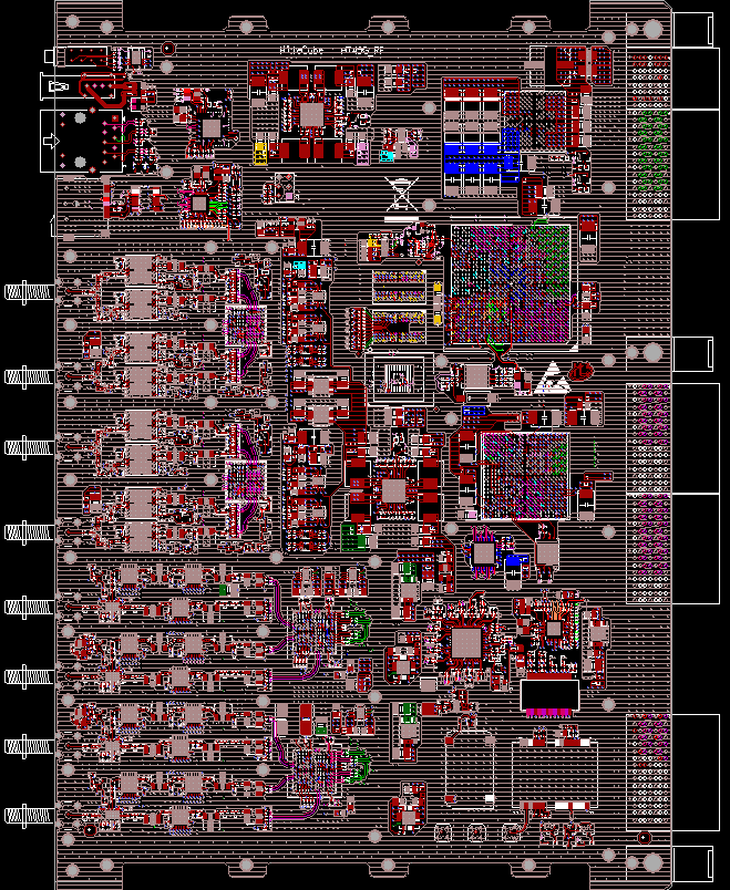
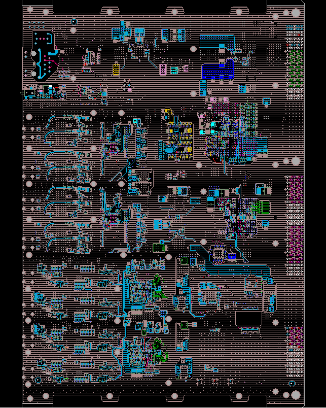
1.According to the VPX architecture, the customer requires there are 8 RF interfaces, indicator lights, USB, network port and TF card. The panel layout is tight. Through evaluation, it is necessary to consider the layout to compress the width of the layout above the Y-axis of RF circuit. the shielding cavity of 2mm width is added to each RF, and the shield cavity of the full version is reserved; the layout is as follows:
2.Due to consider the reliability of the RF signal, 1-2, 15-16 directly used RO4350B, thickness is 10mil, RF traces are processed at the top or bottom layer, no need reference insulation
3.The board of near the top-bottom layer using RO4350B, thickness is 10MIL, if handle it as 1.6MM , there will be only 1.1MM thickness to stack the digital part,it can not meet the requirements of route.after communicating with customers and gave advice, using the ladder process,processing as 16-layer , the top layer only processes the RF circuit, and the digital part traces are all arranged processing in the inner layer , and the top-bottom layer should be irrigated GND copper to dissipate heat and shield.
4.Due to the high heat generated of the RF board , in addition to the RF signal, the rest empty areas of the top-bottom layer are treated as irrigation GND copper, and increase the heat treatment.
5G communication board PCB design case was added in Aug 2019
5G communication board PCB design case has been viewed 467 times
20 More Products from ShenZhen J-Wide Electronics Equipment Co.,Ltd :