Headpcb

Head Electronics Co., Limited (Headpcb), established in 2001, is one of leading quick turn PCB manufacturer who specializes in L2~L30 high-mix, low volume and quickturn prototype PCB for high-tech industries in 30 countries.
Head electronic co.,ltd is a leading Manufacturer specializes in offering PCB(Printed Circuits Board) with years manufacturing experience!
With the helps of an inner Research & Developing Department which is equipped with professional Technicians and the state-of-the-art Equipments, Headpcb is committed to offering quality & precision Printed Circuits Board(Rigid/Flex/Rigid & Flex PCB) for worldwide markets!
Headpcb is your reliable one-stop PCB solution supplier! Fast Prototyping and Quick-Turn Production services are available as well as Large-Volume Production! High-Mix & Low-Volume orders are also welcome!
Headpcb produces its PCB in a High-tech equipment armed factory plants, with the abundant experience and powerful technology in manufacturing PCB (Auto Laminating/Auto V-Scoring/AOI/Routing/Drilling/PTH/Plating/Etching Technologe…), we are able to produce high-density & delicate multilayer quality PCB!
Headpcb’s esteemed customers come from various business fields from every corner of the World! And our products and service are highly appreciated by customers! The customers take delight in cooperating with us as a long-term business partner because our updating technology can meet their requirements and keep them catching the fashion of the PCB field anytime!
Any inquiries and suggestions on Head electronic are cordially welcome!
We can offer all of these benefits…
Technical Supports available anytime.
Prompt Response to quotation requests.
Competitive Pricing.
Full Quality Release available.
For all your Circuit requirements. Friendly & Approachable Service
Headpcb Postings
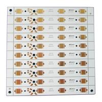
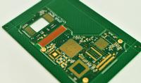
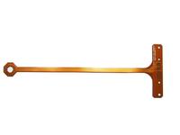
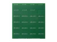
27 products »
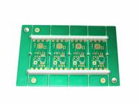
Project Description | Parameters 1 Layer Thickness: 1.2+/-0.1 mm Min Hole Size: 3.175 mm Width/Space: 0....
Project Description | Parameters 2 Layer Thickness: 1.6+/-0.1 mm Min Hole Size: 0.65 mm Width/Space: 0.1...

Project Description | Parameters 4 Layer (1R+2F+1R) Thickness: 0.56+/-0.1 mm Min Hole Size: 0.3 mm Width...
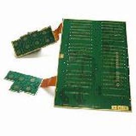
Single Side FPC with Stiffener
Project Description | Parameters 4 Layer Thickness: 0.3+/-0.05 mm Min Hole Size: 0.2 mm Width/Space: 0.1...

Project Description | Parameters 4 Layer (1R+2F+1R) Thickness: 0.56+/-0.1 mm Min Hole Size: 0.3 mm Width/Space...
Project Description | Parameters 4 Layer Thickness: 1.6+/-0.16 mm Min Hole Size: 0.4 mm Width/Space: 0.25mm/0....

Project Description | Parameters 12 Layer Thickness: 2.4+/-0.24 mm Min Hole Size: 0.25 mm Width/Space: 0...
Project Description | Parameters 4 Layer Thickness: 1.8+/-0.18 mm(High Tg S1000-2 Material) Min Hole Size: 0.2 mm...
Project Description | Parameters 4 Layer Thickness: 1.2+/-0.12 mm Min Hole Size: 0.3 mm Width/Space: 0.1...

Project Description | Parameters 4 Layer Thickness: 0.25+/-0.1 mm Min Hole Size: 0.3 mm Width/Space: 0.2...


19 news releases »
How important is Dielectric Constant to your PCB Design?
 Nov 05, 2019 | The board stack-up is probably the most essential piece for ensuring a successful PCB design. Modern high-speed boards require controlled-impedance traces, and whether you are using a simulation tool, a simple calculator, or the back of a napkin, you need to understand your manufacturing process to correlate your impedance calculations. This ensures that your trace widths and dielectric heights match what will actually be manufactured, and eliminates last-minute design changes.
Nov 05, 2019 | Backdrill is the process of creating vias by removing the stub in multilayer_ed printed wiring boards, to allow signals to flow from one layer of the board to another. It is a special craftsmanship of control depth drilling.
Knowledge about PCB Panelization
Nov 05, 2019 | Designing a PCB for automatic assembly and full production runs requires a few design changes from an initial prototype PCB run. Today most PCBs are assembled and tested with automated machines from the data from PCB drawing files. With up to 80% of a new product's cost determined by the first prototype build, avoiding late changes and designing with manufacturing in mind can have a significant impact on the product cost, reliability, and yield of a PCB design. Luckily, if some good choices are made early in the design process, designing a PCB for manufacturing is relatively straight forward with few pitfalls.
Nov 05, 2019 | The basic principle of a press-fit connection is that a contact terminal is pressed into a printed circuit board (PCB). There are two types of press-fit pins – the solid pin with a solid press-in zone and the compliant pin with an elastic press-in zone. In this article, we’ll discuss the elastic press-in zone.
Nov 05, 2019 | 1. The definition of Sideplating
Sideplating is actually the metalization of the board edge in PCB filed. Edge plating、Border plated、plated contour、side metal, these words can be used too to describe same function.
2. Sideplating Process
Drilling - Milling plated Slots - Cleaning - Copper sink
3. Pictures to show the finished board’s sideplating
Which PCB testing method is better for you?
Nov 05, 2019 | Very often, customers ask details about what kind of testing do we use? How do we charge it? Do I have to pay every time or only for the first time? Is this testing safer and better than other one? etc
In this blog, let's discuss the various kind of testing and their advantages and disadvantages. Some of them are mandatory, some of them are optional; Some of them are fast, some are slow; some of them are more reliable, and some not. Hope you will have a better understanding about various kinds testing and make better decision on your next PCB order.
How to improve EMC performance on 8 layer PCB design?
Nov 05, 2019 | 8 Layer PCB Stack-up Guidelines
How to improve EMC performance on 8 layer PCB design?
The following text is reproduced, with permission, from Part 4 of a 6-Part article on PCB Stackup by Henry W. Ott. The original article is available at http://www.hottconsultants.com/tips.html
What is the Advantages of Rigid-Flex PCB?
Nov 05, 2019 | WHAT IS RIGID-FLEX PCB?
Rigid-flex PCB is a printed circuit consisting of both flexible circuit and rigid circuit. This combination is ideal for exploiting the benefits of both flexible and rigid circuits - the rigid circuits can carry all or the bulk of the components, with the flexible sections acting as interconnections between the rigid sections.
Most rigid-flex circuit boards consist of multiple layers of flexible circuit substrates attached to rigid boards externally and/or internally. The flexible substrates are designed to be in a constant state of flex, and are usually formed in a flexed curve during manufacturing or installation. This is dependent upon the design of the application.
Nov 05, 2019 |
Home > > News-Blog > Guideline for wire bonding
Guideline for wire bonding
Tuesday,Jun 12,2018
There are two wire bonding processes that are used, Thermosonic (T/S) Gold Ball Wire Bonding and Ultrasonic (U/S) Aluminum Wedge Wire Bonding. Approximately 90% of all IC Assembly in Semiconductor Packages is manufactured using Gold Ball Bonding process, while Aluminum Wedge Bonding is used to produce about 10% of other Wire Bonding requirements on Printed Circuit Boards (PCB), Printed Circuit Flex (PCF) and other Packages.
Plated Half-Holes(Castellated Holes)
Nov 05, 2019 | Plated half holes(castellated holes)are holes that made off the edge of the boards plated with
copper using a specialized process. It is predominantly used for board-on-board connections, mostly where two printed circuit boards with different technologies are combined.
Through connecting the PCBs together directly, the whole system is considerably thinner than a comparable connection with multi-pin connectors.The plated edges are also useful in producing mini PCB modules.