Industry Directory | Manufacturer's Representative
Camtech Circuits is ISO9001:2008 and UL certificated. We strictly implement ISO9001 quality management system. Each equipment, every process has its own Manual of Engineering Instructions. No matter p
Technical Library | 2011-03-03 16:54:47.0
Most of the electronics industry by now knows about tin whiskers. They know whiskers are slim metallic filaments that emanate from the surface of tin platings. They know these filaments are conductive and can cause shorts across adjacent conductors. And they know that these shorts can cause some really bad failures (see nepp.nasa.gov/whisker/ for a list longer than you need). But, with all of this knowledge, the industry is still struggling on how to predict and prevent these "Nefarious Needles of Pain".
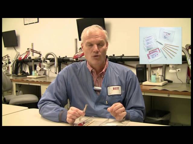
The BEST PCB pad repair repair kit gives you the tools you need for fast modification and repair of PCB circuit pads-no matter what their size. Our online PCB repair training videos, our master instructors along with these materials allows you to mee
Technical Library | 2020-11-15 21:01:24.0
ENIG, electroless nickel immersion gold is now a well-regarded finish used to enhance and preserve the solder-ability of copper circuits. EPIG, electroless palladium immersion gold, is a new surface finish also for enhancing and preserving solder-ability but with the advantage of eliminating Electroless Nickel from the deposit layer. This feature has become increasingly important with the increasing use of high frequeny PWB designs whereby nickel's magnetic properties are detrimental. We examine these two finishes and their respective soldering characteristics as plated and after steam aging and offer an explanation for the performance deviation.
Technical Library | 2017-06-13 17:14:59.0
For tin-rich solder alloys, 200 C (392 F) is an extreme temperature. Intermetallic growth in tin-copper systems is known to occur and is believed to bear a direct relationship to failure mechanisms. This study of morphological changes with time at elevated temperatures was made to determine growth rates of tin-copper intermetallics. Preferred growth directions, rates of thickening, and notable changes in morphology were observed.Each of four tin-base alloys was flowed on copper and exposed to temperatures between 100 C and 200 C for time periods of up to 32 days. Metallographic sections were taken and the intermetallics were examined. Intermetallic layer thickening is characterized by several distinct stages. The initial growth of side plates is extremely rapid and exaggerated. This is followed by retrogression (spheroidization) of the elongated peaks and by general thick-
Industry Directory | Manufacturer
SHENMAO Technology, Inc. supplier of Pb/Pb-free Solder Pastes, Solder Wire, Solder Bar, Flux, BGA Sphere, Bumping Paste/Flux, PCB Plating Anode, PV Ribbon Electronics Assembly Materials, for over 44 years from 10 world locations.
Industry Directory | Manufacturer
Professional, Reliable,High Quality,Low Cost, Rapid Delivery PCB manufacturer
Industry News | 2011-04-06 13:13:52.0
Dow Electronic Materials will showcase its innovative materials for printed circuit boards (PCBs) at this year’s IPC APEX EXPO. Dow will feature a number of its latest products that are tailored to meet the requirements of increasingly complex circuit boards while delivering ever-higher reliability and consistency. Dow’s next-generation of high quality, cost-effective technologies allow customers to meet future market requirements.
Technical Library | 2020-09-02 22:02:13.0
With the adoption of Wafer Level Packages (WLP) in the latest generation mobile handsets, the Printed Circuit Board (PCB) industry has also seen the initial steps of High Density Interconnect (HDI) products migrating away from the current subtractive processes towards a more technically adept technique, based on an advanced modified Semi Additive Process (amSAP). This pattern plate process enables line and space features in the region of 20um to be produced, in combination with fully filled, laser formed microvias. However, in order to achieve these process demands, a step change in the performance of the chemical processes used for metallization of the microvia is essential. In the electroless Copper process, the critical activator step often risks cross contamination by the preceding chemistries. Such events can lead to uncontrolled buildup of Palladium rich residues on the panel surface, which can subsequently inhibit etching and lead to short circuits between the final traces. In addition, with more demands being placed on the microvia, the need for a high uniformity Copper layer has become paramount, unfortunately, as microvia shape is often far from ideal, the deposition or "throw" characteristics of the Copper bath itself are also of critical importance. This "high throwing power" is influential elsewhere in the amSAP technique, as it leads to a thinner surface Copper layer, which aids the etching process and enables the ultra-fine features being demanded by today's high end PCB applications. This paper discusses the performance of an electroless Copper plating process that has been developed to satisfy the needs of challenging amSAP applications. Through the use of a radical predip chemistry, the formation, build up and deposition of uncontrolled Pd residues arising from activator contamination has been virtually eradicated. With the adoption of a high throwing power Copper bath, sub 30um features are enabled and microvia coverage is shown to be greatly improved, even in complex via shapes which would otherwise suffer from uneven coverage and risk premature failure in service. Through a mixture of development and production data, this paper aims to highlight the benefits and robust performance of the new electroless Copper process for amSAP applications
Industry News | 2018-11-27 14:03:14.0
Super PCB is pleased to announce that it offers a variety of quality PCB surface finishes. PCB surface finish is the coating between the PCB and components that provides a solderable surface for components and protects the exposed copper circuitry.