New Equipment | Solder Materials
eFlux Selection: Rosin Based Flux for Lead-Free Wave Soldering NS-F850. NS-F850 ensures excellent wetting of all PCB and component substrates to deliver maximum through hole fill and facilitates the solder drainage that ensures minimum bridges an
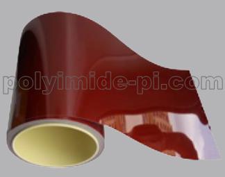
Polyimide Film Stiffener ( Brown/Black) Halogen free Polyimide film stiffener is made of high heat resistant and high adhesive adhesive coating on PI film substrate,and the thickness is from 1mil to 10mil. The excellent properties of heat bonded to e
Parmod�, Parelec Inc�s patented conductive ink technology, enables the formation of continuous-phase pure metallic conductors at relatively low temperature�making them suitable for application to polymer substrates. Parmod� inks, pastes and toners ca
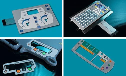
Molex's membrane switches provide durable, lightweight and low-profile options for integrating user interfaces and electronic components into a variety of applications including medical, industrial and commercial products. Molex standard membrane s
Industry News | 2012-01-13 12:42:50.0
Nihon Superior Co. Ltd., a supplier of advanced soldering materials to the global market, announces that Senior Technical Advisor Keith Sweatman will present “The Stability of Cu6Sn5 in the Formation and Performance of Lead-free Solder Joints” at the SMTA Pan Pacific Microelectronics Symposium.
New Equipment | Solder Materials
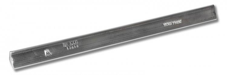
SN100C is a lead-free solder alloy developed by Nihon Superior in Japan that is comprised of tin-copper-nickel + germanium. SN100C offers user-friendly properties and has been proven in commercial production since 1999. The result of these advantages
Technical Library | 2017-11-22 12:38:51.0
The use of copper foils laminated to polyimide (PI) as flexible printed circuit board precursor is a standard practice in the PCB industry. We have previously described[1] an approach to very thin copper laminates of coating uniform layers of nano copper inks and converting them into conductive foils via photonic sintering with a multibulb conveyor system, which is consistent with roll-to-roll manufacturing. The copper thickness of these foils can be augmented by electroplating. Very thin copper layers enable etching fine lines in the flexible circuit. These films must adhere tenaciously to the polyimide substrate.In this paper, we investigate the factors which improve and inhibit adhesion. It was found that the ink composition, photonic sintering conditions, substrate pretreatment, and the inclusion of layers (metal and organic) intermediate between the copper and the polyimide are important.
Technical Library | 2021-11-03 16:52:47.0
This paper proposes the integration of pulsed photonic sintering into multi-material additive manufacturing processes in order to produce multifunctional components that would be nearly impossible to produce any other way. Pulsed photonic curing uses high power Xenon flash lamps to thermally fuse printed nanomaterials such as conductive metal inks. To determine the feasibility of the proposed integration, three different polymer additive manufacturing materials were exposed to typical flash curing conditions using a Novacentrix Pulseforge 3300 system. FTIR analysis revealed virtually no change in the polymer substrates, thus indicating that the curing energy did not damage the polymer. Next, copper traces were printed on the same substrate, dried, and photonically cured to establish the feasibility of thermally fusing copper metal on the polymer additive manufacturing substrates. Although drying defects were observed, electrical resistivity values ranging from 0.081 to 0.103 Ω/sq. indicated that high temperature and easily oxidized metals can be successfully printed and cured on several commonly used polymer additive manufacturing materials. These results indicate that pulsed photonic curing holds tremendous promise as an enabling technology for next generation multimaterial additive manufacturing processes.
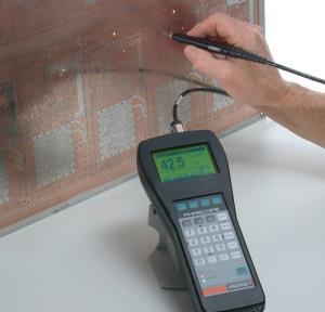
New Equipment | Test Equipment
The hand-held PHASCOPE® PMP10 is ideally suited for quality control in the electroplating and printed circuit board (PCB) industries. Because the instrument employs the phase-sensitive eddy current method (ISO 21 968), it allows the measurement of me
Industry News | 2023-09-04 13:25:54.0
Heraeus Electronics, an expert in materials and matched material solutions for the electronics packaging, is one of five partners in the three-year joint project "KuSIn - Copper sinter processes using induction heating for electromobility applications", funded by the German Federal Ministry of Economic Affairs and Climate Action (BMWK).