Suitable for direct connection of solid. stranded or fine standed machine tool wire, as well as with crimped ferrules, pin terminals or tip bonded wire. All products designed in accordance with IEC60947, IEC60079, UL1059, UL486E, CSA C22.2 No.158 sta
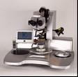
For Wire Bonding (Wedge and Ball Bonding)
Technical Library | 2014-12-11 18:00:09.0
The growth of portable and wireless products is driving the miniaturization of packages resulting in the development of many types of thin form factor packages and cost effective assembly processes. Wire bonded packages using conventional copper lead frame have been used in industry for quite some time. However, the demand for consumer electronics is driving the need for flip chip interconnects as these packages shorten the signals, reduce inductance and improve functionality as compared to the wire bonded packages. The flip chip packages have solder bumps as interconnects instead of wire bonds and typically use an interposer or organic substrate instead of a metal lead frame (...) The paper provides a general overview of typical defects and failure modes seen in package assembly and reviews the efforts needed to understand new failure modes during package assembly. The root cause evaluations and lessons learned as the factory transitioned to thin form factor packages are shared
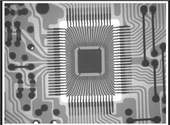
High accuracy inspection guarantees reliable defect detection of die bonds, ball-to-wedge, wedge-to-wedge and security bonds Inspection of minimal wire thicknesses up to 15 µm Reliable differentiation of wire courses Recognition of defective bon
Counterfeit components are defined as; substitutes or unauthorised copies of a product, a product used in which the materials used or the performance of the product has changed without notice, or a substandard component misrepresented by the supplier
.JPG)
Used SMT Equipment | Adhesive Dispensers
Asymtek Millennium 600 Epoxy Dispenser For Sale Vintage 1998 Integrated mass flow calibration system automatically compensates for changes in fluid viscosity Full temperature control of fluid delivery with closed-loop substrate heating to
Used SMT Equipment | Semiconductor & Solar
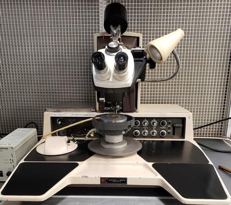
Becoming available soon; K&S 4124 Wire Bonding Machine currently in production to be removed in complete working condition. Contact: Assured Technical Service LLC Minneapolis, MN 55441 AssuredTechnicalServiceLLC@Gmail.com FOB Origin. The
Complex functions are compressed on ever less room while simultaneously an enhancement in performance must be obtained. With coated Bonding pads in various designs Heraeus Materials Technology offers customer oriented solutions that aid the increas
Wire-bonding Technician: Capable of programming, repair and support automatic K&S 1419 wire bonders and MECH-EL /MEI manual bonders, among with other assy equipment. Familiarity with HYBRID assemblies in a semiconductors environment. SPC knowlege.
Technical Library | 2020-08-27 01:22:45.0
Initially adopted internal specifications for acceptance of printed circuit boards (PCBs) used for wire bonding was that there were no nodules or scratches allowed on the wirebond pads when inspected under 20X magnification. The nodules and scratches were not defined by measurable dimensions and were considered to be unacceptable if there was any sign of a visual blemish on wire-bondable features. Analysis of the yield at a PCB manufacturer monitored monthly for over two years indicated that the target yield could not be achieved, and the main reasons for yield loss were due to nodules and scratches on the wirebonding pads. The PCB manufacturer attempted to eliminate nodules and scratches. First, a light-scrubbing step was added after electroless copper plating to remove any co-deposited fine particles that acted as a seed for nodules at the time of copper plating. Then, the electrolytic copper plating tank was emptied, fully cleaned, and filtered to eliminate the possibility of co-deposited particles in the electroplating process. Both actions greatly reduced the density of the nodules but did not fully eliminate them. Even though there was only one nodule on any wire-bonding pad, the board was still considered a reject. To reduce scratches on wirebonding pads, the PCB manufacturer utilized foam trays after routing the boards so that they did not make direct contact with other boards. This action significantly reduced the scratches on wire-bonding pads, even though some isolated scratches still appeared from time to time, which caused the boards to be rejected. Even with these significant improvements, the target yield remained unachievable. Another approach was then taken to consider if wire bonding could be successfully performed over nodules and scratches and if there was a dimensional threshold where wire bonding could be successful. A gold ball bonding process called either stand-off-stitch bonding (SSB) or ball-stitch-on-ball bonding (BSOB) was used to determine the effects of nodules and scratches on wire bonds. The dimension of nodules, including height, and the size of scratches, including width, were measured before wire bonding. Wire bonding was then performed directly on various sizes of nodules and scratches on the bonding pad, and the evaluation of wire bonds was conducted using wire pull tests before and after reliability testing. Based on the results of the wire-bonding evaluation, the internal specification for nodules and scratches for wirebondable PCBs was modified to allow nodules and scratches with a certain height and a width limitation compared to initially adopted internal specifications of no nodules and no scratches. Such an approach resulted in improved yield at the PCB manufacturer.

.gif)