Events Calendar | Mon Dec 02 00:00:00 EST 2019 - Mon Dec 02 00:00:00 EST 2019 | ,
Webinar: QFN/LGA Design, Assembly Process Issues & Reliability Failures
Used SMT Equipment | AOI / Automated Optical Inspection
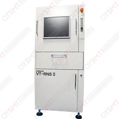
OMRON AOI VT-RNS2-L Omron AoiVT-RNSⅡ parameters Hardware part LSIZE Image signal input part Camera 3CCD camera Lighting series Ring LED (R.G.B) Image resolution 10, 15, 20um Mechanism part Transmission method Belt transmission method Producti
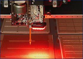
Online AOI For SMT from SZTech with AI algorithm. What is the AI algorithm SMT Online AOI? AI intelligent programming Automatically select solder joints and set parameters without importing CAD, Gerber, or other files. Online/Offline programm
Technical Library | 2023-09-16 06:27:24.0
Vacuum reflow ovens are the best way to solder SMD components. They create a controlled environment that prevents oxidation and improves solder joint quality.
ACI Technologies employs personnel that are Master IPC Trainers and Certified IPC Trainers for all IPC inspection standards. Visual Inspection Services ACI Technologies employs personnel that are Master IPC Trainers and Certified IPC Trainers for a

Parts & Supplies | Pick and Place/Feeders
The definition of SMT SMT is the surface assembly technology,surface mount technology(surface mount technology)(Surface Mounted Technology abbreviation),is currently the most popular electronic assembly industry,a technology and technology. What a
Events Calendar | Tue Apr 21 00:00:00 EDT 2020 - Thu Apr 23 00:00:00 EDT 2020 | Amsterdam, Netherlands
Electronics in Harsh Environments Conference
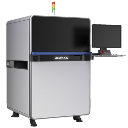
Online SMT THT DIP AOI Machine AIS50X Principle Photograph the same board on the move with the upper and lower high precision cameras. Process image with Convolutional Neural Network (CNN) algorithm. Intelligently judge defects of components and sol
Hear what attendees had to say about the Electronics in Harsh Environments Conference. Start planning your participation for the 2020 event: 21-23 April 2020 | Amsterdam, Netherlands https://www.smta.org/harsh
Technical Library | 2019-09-03 17:06:09.0
Both optical and scanning electron microscopy (SEM) are powerful tools for failure analysis in electronics and are used for low and high magnification examination. This article will provide detailed, step by step information for examining solder joints.