China ISO factory of emi rf shielding can emi shielding cover for PCB board Various material available :SPTE ,Nickel silver ,Copper etc.... 5 days for prototype 7-15 days for progressive die Tape reel , plastic tray Any RFQ please send mail t

New Equipment | Soldering - Other
PARENTNashik offers resistance spot welding Spares, consumables & accessories weldparts for portable welders, spot welding guns, projection & seam welder, machines. Spot welding electrodes, cap tips, bend electrodes, double bend electrodes, shanks,
New Equipment | Fabrication Services
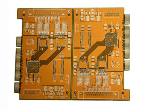
Gold Finger PCB No of layer: 6 layer Material: FR-4, TG170 Thickness: 1.6mm Copper thickness: 35um copper/1oz Yellow Solder Mask Surface finishing: ENIG, gold 0.05-0.1um, Nickel 3-5um Special technology: gold finger/Edge connector plating, go

Paramount Enterprises with a renowned brand PARENTNashik is an ISO 9001:2015 certified company, listed in major leading manufacturers, suppliers & exporters of resistance spot welding consumables, spares, weldparts in Nashik – India. PARENTNashik is
Technical Library | 2021-07-06 21:20:38.0
The evolution of internet-enabled mobile devices has driven innovation in the manufacturing and design of technology capable of high-frequency electronic signal transfer. Among the primary factors affecting the integrity of high-frequency signals is the surface finish applied on PCB copper pads – a need commonly met through the electroless nickel immersion gold process, ENIG. However, there are well-documented limitations of ENIG due to the presence of nickel, the properties of which result in an overall reduced performance in high-frequency data transfer rate for ENIG-applied electronics, compared to bare copper.
Industry Directory | Manufacturer
Nihon has been a leader in soldering and brazing since 1966. Nihon manufactures SMT solder joining materials e.g. lead-free solder (SN100C:Sn-Cu-Ni-Ge etc): solder paste, solder spheres, flux cored solder wire, solder bar, etc.
Technical Library | 2010-07-08 19:49:59.0
Aging characteristics of new lead free solder alloys are in question by many experts because of higher amount of tin’s effect on the diffusion of other metals, primarily copper, to create undesirable boundary intermetallics over long periods of time and even moderately elevated temperatures. A primary layer of intermetallics, Cu6Sn5 forms as the liquid solder makes contact with the solid copper substrate. This reaction however ceases as the solder temperature falls below that of liquidus. A secondary intermetallic Cu3Sn1, an undesirable weak and brittle layer, is thought to form over time and may be accelerated by even mildly elevated temperatures in electronic modules such as laptops under power. This project was designed to quantify the growth rate of Cu3Sn1 over an extended period of time in a thermal environment similar to a laptop in the power on mode.
Technical Library | 2023-01-10 20:15:42.0
Over the past years there has been consistent growth in the use of electroless nickel / immersion gold (ENIG) as a final finish. The finish is now frequently being used for PBGA, CSP, QFP and COB and more recently gathered considerable interest as a low cost under-bump metallization for flip chip bumping application. One of the largest users for this finish has been the telecommunication industry, were millions of square meters of PCBs with ENIG have been successfully used. The nickel layer offers advantages such as multiple soldering cycles and hand reworks without copper dissolution being a factor. The nickel also acts as a reinforcement to improve through-hole and blind micro via thermal integrity. In addition the nickel layer offers advantages such as co-planarity, Al-wire bondability and the use as contact surface for keypads or contact switching. Especially those pads, which are not covered by solder need a protective coating in corrosive environment – such as high humidity or pollutant gas.

Great Lakes Engineering boasts over 20 years in chemical etching technology. In essence, this is the process of printing (photo-plotting) a pattern on a metal foil and immersing it in a precise combination of chemistry in order to eat through (etch t

At Barry: custom requests are common and welcome. We enjoy the challange. Extensive capabilities, wide material selection and state-of-the-art equiptment (including in-house plating and machining) ensure we can deliver a component fitting your exact