LSMO-105 fastest and most reliable stencil inspection machine www.aoivision.com
New Equipment | Solder Paste Stencils
PNC Inc. uses LPKF Laser Technology to manufacture SMT Solder paste stencil, high tolerance aperture openings with superior registration for it’s solder paste stencils. With it’s 4 mil beam diameter, our Laser is capable of cutting small aperture ope
Used SMT Equipment | Screen Printers
Two sets of blades with some poly inserts and a small roll of Ekra wiper paper; 10 support pins; A removable tool plate that can be adjusted by the leveling feet on the bottom. Was usedt to print 150um apertures so I believe it’s better than most use

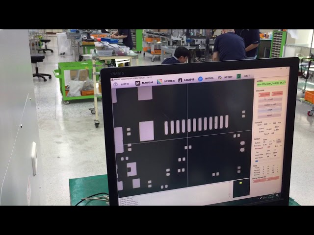
World's leading solder paste stencil & emulsion screen inspection system. Used by both stencil/screen fabricators and users to detect errors BEFORE production, eliminating costly rework, scrap and delays. Supports E-form, laser cut, chem etch, hybrid
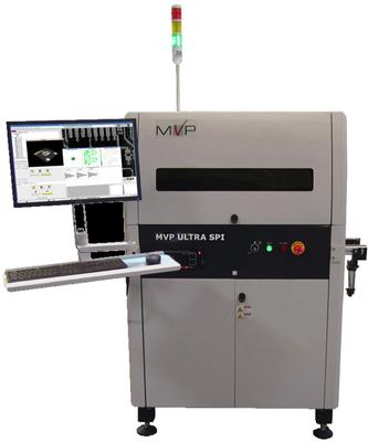
MVP’s enhanced Ultra SPI Solder Paste Inspection systems deploy our patented 3D technologies along with MVPs trusted AOI capabilities. Utilizing MVP’s patented technology, 3D Solder Paste Inspection (SPI) can be performed on paste for apertures as sm
New Equipment | Cleaning Agents
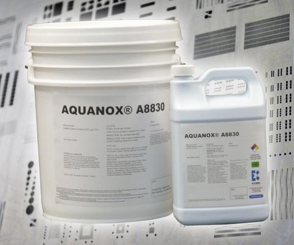
AQUANOX® A8830 is a mild formulation that does not damage stencils and is highly effective at removing all types of solder pastes (water soluble, rosin, and no-clean) from fine pitch apertures. AQUANOX A8830 is a low odor cleaner that can be used
New Equipment | Solder Paste Stencils
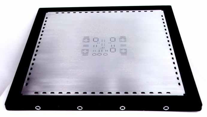
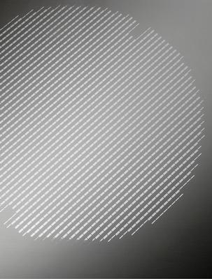
Laser cut stainless steel stencil for solder paste printing on wafer. Wafer bumping stencils are characterized by a high number of apertures which lie close together in the size of 90µm x 110µm. A package density of up to 250000 openings is not unus
Technical Library | 2023-07-25 16:42:54.0
Printing solder paste for very small components like .3mm pitch CSP's and 01005 Chip Components is a challenge for the printing process when other larger components like RF shields, SMT Connectors, and large chip or resistor components are also present on the PCB. The smaller components require a stencil thickness typically of 3 mils (75u) to keep the Area Ratio greater than .55 for good paste transfer efficiency. The larger components require either more solder paste height or volume, thus a stencil thickness in the range of 4 to 5 mils (100 to 125u). This paper will explore two stencil solutions to solve this dilemma. The first is a "Two Print Stencil" option where the small component apertures are printed with a thin stencil and the larger components with a thicker stencil with relief pockets for the first print. Successful prints with Keep-Outs as small as 15 mils (400u) will be demonstrated. The second solution is a stencil technology that will provide good paste transfer efficiency for Area Ratio's below .5. In this case a thicker stencil can be utilized to print all components. Paste transfer results for several different stencil types including Laser-Cut Fine Grain stainless steel, Laser-Cut stainless steel with and w/o PTFE Teflon coating, AMTX E-FAB with and w/o PTFE coating for Area Ratios ranging from .4 up to .69.
Industry News | 2018-10-18 10:24:05.0
The Design Principles of Stencil Apertures