Industry Directory | Manufacturer
PRINTED CIRCUIT BOARDS MANUFACTURER located in Guangdong China 2-14 LAYER VARIOUS TYPES OF FINISHING UL E150111 ISO9001; ISO/TS16949:2002; ISO14001:2004 5S and RoHS CUSTOMER ORIENTATED BE THE CUSTOMER'S SUPPLYING PARTNER
Industry Directory | Manufacturer
PCBGOGO offers ISO9001:2015 standard PCB Fabrication & Assembly, from prototype to mass production. Quick-turn 24 hours, $5 for 10 PCBs, Min. $30 for PCB assembly. Start your inquiry and order now: service@pcbgogo.com
New Equipment | Assembly Services
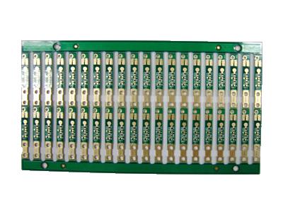
Material: FR-4 Layer: 2 Board thickness: 1.0 mm Copper: 1 oz Surface finish: LEAD FREE HASL Min through hole: 0.3 mm Min line width: 0.3 mm Min line space:0.3 mm Soldermask color: Green Silkscreen color: white RoHS certificate
New Equipment | Assembly Services
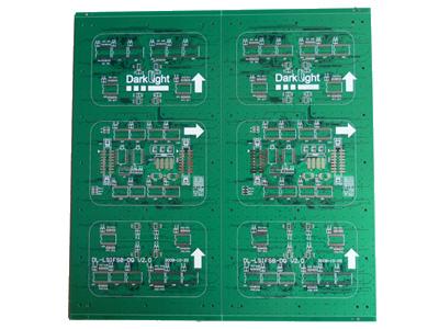
Material: FR-4 Layer: 2 Board thickness: 1.0 mm Copper: 1 oz Surface finish: LEAD FREE HASL Min through hole: 0.3 mm Min line width: 0.3 mm Min line space:0.3 mm Soldermask color: Green Silkscreen color: white RoHS certificate
Technical Library | 2023-02-13 19:23:18.0
Spontaneously forming tin whiskers, which emerge unpredictably from pure tin surfaces, have regained prevalence as a topic within the electronics research community. This has resulted from the ROHS-driven conversion to "lead-free" solderable finish processes. Intrinsic stresses (and/or gradients) in plated films are considered to be a primary driving force behind the growth of tin whiskers. This paper compares the formation of tin whiskers on nanocrystalline and conventional polycrystalline copper deposits. Nanocrystalline copper under-metal deposits were investigated, in terms of their ability to mitigate whisker formation, because of their fine grain size and reduced film stress. Pure tin films were deposited using matte and bright electroplating, electroless plating, and electron beam evaporation. The samples were then subjected to thermal cycling conditions in order to expedite whisker growth. The resultant surface morphologies and whisker formations were evaluated.
Technical Library | 2021-01-28 01:55:00.0
Printed circuit board surface finishes are a topic of constant discussion as environmental influences, such as the Restriction of Hazardous Substances (RoHS) Directive or technology challenges, such as flip chip and 01005 passive components, initiate technology changes. These factors drive the need for greater control of processing characteristics like coplanarity and solderability, which influence the selection of surface finishes and impact costs as well as process robustness and integrity. The ideal printed circuit board finish would have good solderability, long shelf life, ease of fabrication/processing, robust environmental performance and provide dual soldering/wirebonding capabilities; unfortunately no single industry surface finish possesses all of these traits. The selection of a printed circuit board surface finish is ultimately a series of compromises for a given application.
New Equipment | Fabrication Services
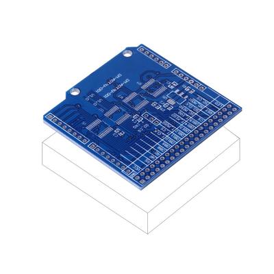
Quantity: 10pcs Lead Time: 9 working days Number of layers: 2 layers Max board dimensions: 6300x3900mils/160x100mm Material: R-4, Tg130 Finished Thickness: 63mil/1.6mm Min Trace/space: 4mil/0.1mm Min.Holes size: 12mil/0.3mm Co
New Equipment | Fabrication Services
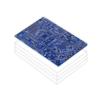
Quantity: 10pcs Lead Time: 9 working days Number of layers: 4 layers Max board dimensions: 6300x3900mils/160x100mm Material: R-4, Tg130 Finished Thickness: 63mil/1.6mm Min Trace/space: 4mil/0.1mm Min.Holes size: 12mil/0.3mm Co
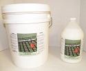
New Equipment | ESD Control Supplies
AF-7232 can be applied over non ESD tiles/paint and ESD tiles/paint to protect, increase longevity, and maintain the ESD properties. Eco-Stat Green formula meets and exceeds Massachusetts and California state regulatory guidelines in order to ensure

http://www.quickshotxrf.com Quickshot XRF Sales Representative gives a brief overview of the Handheld X-ray Fluorescence technology. Visit the QSX website for details on the system, which provides a testing solution for hazardous substance detection