Industry News | 2010-02-17 18:45:59.0
The SMTA International Technical Committee invites you to submit an abstract for the 2010 conference. Short course descriptions are also being solicited.
Industry News | 2010-05-07 16:01:14.0
New this year! The SMTA International Technical Committee invites you to participate in a poster session at SMTA International. Poster sessions are presented on the show floor and are a great way to present current research and results in a concise manner without requiring a technical paper.
Industry News | 2021-02-25 13:34:06.0
The best technical conference paper of IPC APEX EXPO 2021 has been selected. Voted on through a ballot process by members of the IPC APEX EXPO Technical Program Committee, the paper authors will be recognized during show opening remarks on Tuesday, March 9.
Industry News | 2011-03-31 11:54:23.0
Over the past few years, pad cratering has become a vexing problem in lead-free assemblies, largely attributed to problems with the resin used to make a printed board. To help industry eliminate the defect and, at the same time, cut costs, IPC — Association Connecting Electronics Industries® has released IPC-9708, Test Methods for Characterization of PCB Pad Cratering.
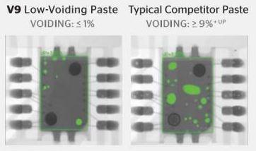
New Equipment | Solder Materials
V9 No Clean solder paste is formulated for near-zero voiding on BGA, BTC and LED soldering applications. Significant void reduction achievable on all surface finishes including ENIG, ImSn and OSP. V9 exhibits stable print performance on fine feature
Technical Library | 2017-11-08 23:22:04.0
Due to the ongoing trend towards miniaturization of power components, the need for increased thermal conductivity of solder joints in SMT processes gains more and more importance. Therefore, the role of void free solder joints in power electronics becomes more central. Voids developed during soldering reduce the actual thermal transfer and can cause thermal damage of the power components up to their failure. For this reason, the company has developed a new technique to minimize the formation of these voids during the soldering process.
Technical Library | 2021-04-21 19:28:30.0
Voids affect the thermal characteristics and mechanical properties of a solder joint, thereby affecting the reliability of the solder interconnect. The automotive sector in particular is requiring the mitigation of solder voids in various electronic control modules to the minimum possible level. Earlier research efforts performed to decrease voids involved varying the reflow profile, paste deposit, paste alloy composition, stencil aperture, and thickness.
Events Calendar | Tue Nov 05 00:00:00 EST 2019 - Tue Nov 05 00:00:00 EST 2019 | North Billerica, Massachusetts USA
Free Vacuum Reflow Workshop
Technical Library | 2019-08-07 22:56:45.0
The requirement to reconsider traditional soldering methods is becoming more relevant as the demand for bottom terminated components (QFN/BTC) increases. Thermal pads under said components are designed to enhance the thermal and electrical performance of the component and ultimately allow the component to run more efficiently. Additionally, low voiding is important in decreasing the current path of the circuit to maximize high speed and RF performances. The demand to develop smaller, more reliable, packages has seen voiding requirements decrease below 15 percent and in some instances, below 10 percent.Earlier work has demonstrated the use of micro-fluxed solder preforms as a mechanism to reduce voiding. The current work builds upon these results to focus on developing an engineered approach to void reduction in leadless components (QFN) through increasing understanding of how processing parameters and a use of custom designed micro-fluxed preforms interact. Leveraging the use of a micro-fluxed solder preform in conjunction with low voiding solder paste, stencil design, and application knowhow are critical factors in determining voiding in QFN packages. The study presented seeks to understand the vectors that can contribute to voiding such as PCB pad finish, reflow profile, reflow atmosphere, via configuration, and ultimately solder design.A collaboration between three companies consisting of solder materials supplier, a power semiconductor supplier, and an electronic assembly manufacturer worked together for an in-depth study into the effectiveness of solder preforms at reducing voiding under some of the most prevalent bottom terminated components packages. The effects of factors such as thermal pad size, finish on PCB, preform types, stencil design, reflow profile and atmosphere, have been evaluated using lead-free SAC305 low voiding solder paste and micro-fluxed preforms. Design and manufacturing rules developed from this work will be discussed.
Technical Library | 2018-09-26 20:33:26.0
Bottom terminated components, or BTCs, have been rapidly incorporated into PCB designs because of their low cost, small footprint and overall reliability. The combination of leadless terminations with underside ground/thermal pads have presented a multitude of challenges to PCB assemblers, including tilting, poor solder fillet formation, difficult inspection and – most notably – center pad voiding. Voids in large SMT solder joints can be difficult to predict and control due to the variety of input variables that can influence their formation. Solder paste chemistries, PCB final finishes, and reflow profiles and atmospheres have all been scrutinized, and their effects well documented. Additionally, many of the published center pad voiding studies have focused on optimizing center pad footprint and stencil aperture designs. This study focuses on I/O pad stencil modifications rather than center pad modifications. It shows a no-cost, easily implemented I/O design guideline that can be deployed to consistently and repeatedly reduce void formation on BTC-style packages.