Industry Directory | Consultant / Service Provider / Manufacturer
Tropical Stencil is dedicated to providing the highest quality Laser Cut Stencils; with our rapid response, you will have your Stencil delivered on-time.
Industry Directory | Consultant / Service Provider
Smart CAD Service can provide you with solutions to your SMT CAD Designs and economical solutions to cost reduction. We can help you reduce capital costs of infrastructure.
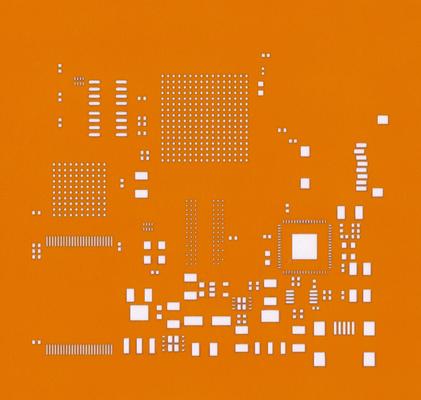
New Equipment | Solder Paste Stencils
For the DIYer, hobbyist or technical researcher there are times where all you need is a simple means to apply solder paste for SMT devices for a few simple boards. In those cases a plastic SMT stencil may be the right solution. Eliminate the tedious
New Equipment | ESD Control Supplies
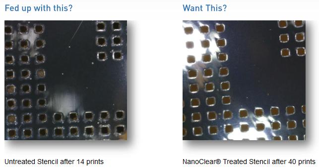
High performance fluxophobic stencil treatments wipes Enhance your stencil performance in seconds! Aculon is pleased to announce the launch of their latest generation of stencil coating technology. Aculon’s proprietary technology treats the undersi
Electronics Forum | Thu Apr 12 09:50:51 EDT 2007 | pjc
There have been many designs of apertures for 0402, round, home plate, inverted home plate and various reduction amounts for square or rectangular apertures. What works best for a given application depends on PCB design, solder land finish, stencil t
Electronics Forum | Thu Oct 30 15:36:18 EDT 2008 | grantp
Hi, Sounds like your engineer does not know what he's doing. We have developed and built hundreds of thousands of boards with normal square pads for 0402, and we just use a 5 thou stencil with 5% reduction and it works well. Decoupling? What is tha
Industry News | 2013-01-19 07:46:16.0
Information that inspires innovation is center-stage for design, printed boards, electronics assembly, test and printed electronics
Industry News | 2016-10-25 09:47:33.0
Learn about SMT assembly from SME Phil Zarrow in Chicago
Technical Library | 2018-09-26 20:33:26.0
Bottom terminated components, or BTCs, have been rapidly incorporated into PCB designs because of their low cost, small footprint and overall reliability. The combination of leadless terminations with underside ground/thermal pads have presented a multitude of challenges to PCB assemblers, including tilting, poor solder fillet formation, difficult inspection and – most notably – center pad voiding. Voids in large SMT solder joints can be difficult to predict and control due to the variety of input variables that can influence their formation. Solder paste chemistries, PCB final finishes, and reflow profiles and atmospheres have all been scrutinized, and their effects well documented. Additionally, many of the published center pad voiding studies have focused on optimizing center pad footprint and stencil aperture designs. This study focuses on I/O pad stencil modifications rather than center pad modifications. It shows a no-cost, easily implemented I/O design guideline that can be deployed to consistently and repeatedly reduce void formation on BTC-style packages.
Technical Library | 2014-03-13 15:25:01.0
A student competition paper at Budapest University of Technology And Economics, Department of Electronics Technology gives background, covers stencil design and discusses stencils intended for pin in paste application. The stencil applied for depositing the solder paste is a thin, 75–200 µm thick metal foil, on which apertures are formed according to the solder pads on the printed circuit board. Stencil printing provides a fast, mass solder paste deposition process; relatively expensive, appropriate and recommended for mass production.
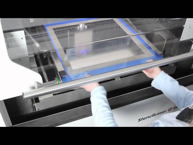
SMT Stencil Production with the LPKF StencilLaser G 6080 The LPKF StencilLaser G 6080 is a highly productive and precise SMT stencil laser cutting system. Learn more: http://www.lpkf.com/products/smt-stencils/cutting-smt-stencils-and-microparts.htm?u
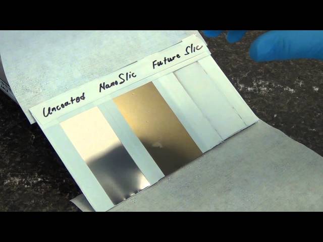
NanoSlic™ Gold is our top of the line spray on coating applied to our UltraSlic™ solder paste stencil, which gives previously unseen performance benefits in transfer efficiency. The NanoSlic™ Gold coating also gives the benefits of improved under-ste
Events Calendar | Wed May 31 00:00:00 EDT 2023 - Wed May 31 00:00:00 EDT 2023 | Holtsville, New York USA
Long Island Chapter Meeting: Fine Feature Paste Printing, Stencil Design and Solder Technology
Career Center | Bangalore, India | Engineering,Maintenance,Production,Technical Support
SMT Stencil designing & Knowledge of full SMT process software known CAD/CAM -circuit CAM Pro 7.3,GC Power station, GCCAM Edit,Auto CAD, Fault finding of Electronic Boards & Servicing electronic machines.
Career Center | , | Engineering,Production
Project Management, SMT Process Engineering
SMTnet Express, September 27, 2018, Subscribers: 31,354, Companies: 11,055, Users: 25,237 Assessing the Effectiveness of I/O Stencil Aperture Modifications on BTC Void Reduction Carlos Tafoya, Gustavo Ramirez, Timothy O'Neill; AIM Solder Bottom
Heller 公司 | http://hellerindustries.com.cn/Vacuum-Void-Reduction-Reflow.pdf
. Half of the population of test vehicles then were re-processed (reflowed) using vacuum reflow. Transmission x-ray inspection showed a significant reduction in solder voiding after vacuum processing
Heller Industries Inc. | https://hellerindustries.com/wp-content/uploads/2018/07/Vacuum-Void-Reduction-Reflow.pdf
. Half of the population of test vehicles then were re-processed (reflowed) using vacuum reflow. Transmission x-ray inspection showed a significant reduction in solder voiding after vacuum processing