Industry Directory | Manufacturer
SAFE-PCB Group is a global leading provider of time-critical and technologically complex PCBs, attractive for small and medium volume quick-turn orders. We provide 2-hour images for validation, same day production, and wide range.
New Equipment | Test Equipment
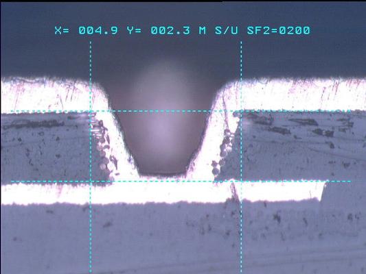
Military-style laboratory services to validate bare boards for product assurance. Testing for delamination, voids, copper thickness, hole quality, proper stack-up, etc. Customer receives all cross-section pucks, boards and laboratory report with reco
MLT provides microvia laser drilling services for both rigid and flexible circuit board manufacturers. MLT is a leader in HDI drilling and design consulting to minimize drilling costs. All IPC high density microvia types are supported in most any s
Electronics Forum | Sat Jun 06 15:11:17 EDT 2009 | ysutariya
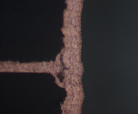
Was this a lead-free capable material that fits into IPC 4101/126 or /129, like an Isola 370HR? I would not be surprised because from the picture I think I can see resin underneath the lifted copper, which is an interlaminate separate. This is a
Electronics Forum | Sun Aug 23 11:30:51 EDT 2009 | ysutariya
I think you're getting steered in the wrong direction, with the exception of DaveF's link. By the way, I'm a PCB fabricator, just to avoid any backlash. IPC 4101 is the IPC guideline for raw materials. It has 6 slash sheets for lead-free capable
Industry News | 2024-04-29 08:34:13.0
At IPC APEX EXPO 2024 in Anaheim, Calif., five competitors squared off to determine who was the best of the best at PCB design.
Industry News | 2011-01-10 19:20:49.0
Plans are ramping up for IPC APEX EXPO™, April 10–14 in Las Vegas, aimed at meeting the needs of the engineers, PCB designers and manufacturing wizards who are tasked with bringing today’s consumer, industrial and high-reliability electronic products to life. With a focus on education, IPC will bring industry experts from around the world to lead 50 half-day professional development courses covering critical topics in design, PCB manufacturing, electronics assembly and test — supporting electronics manufacturers as they develop the next generation of electronics.
Technical Library | 2012-09-20 21:45:38.0
First published in the 2012 IPC APEX EXPO technical conference proceedings. An evaluation of four FR4 laminates in commonly used stack-ups was done to determine their survivability for the Pb-free HASL process followed by a worst case Pb-free manufacturin
Events Calendar | Wed Jul 26 00:00:00 EDT 2017 - Wed Jul 26 00:00:00 EDT 2017 | Chicago, Illinois USA
IPC Technical Education - Best Practices in Design
Events Calendar | Tue Jul 11 00:00:00 EDT 2023 - Tue Jul 11 00:00:00 EDT 2023 | Oshkosh, Wisconsin USA
Wisconsin Chapter In-Person Event: PCB Workshop and PCB Plant Tour
Manufacture and Characterization of a Novel Flip-Chip Package Z-interconnect Stack-up with RF Structures Manufacture and Characterization of a Novel Flip-Chip Package Z-interconnect Stack-up with RF Structures More and more chip packages need
Multilayer PCB Stackup Planning Multilayer PCB Stackup Planning Planning the multilayer PCB stackup configuration is one of the most important aspects in achieving the best possible performance of a product. A correctly stacked PCB substrate can
IPC is the trade association for the printed wiring board and electronics assembly industries.
Training Provider / Events Organizer / Association / Non-Profit
3000 Lakeside Drive, 309 S
Bannockburn, IL USA
Phone: 847-615-7100