Industry Directory | Manufacturer
Nepes offers flip chip solutions ranging from wafer bumping to advanced packaging and testing for IC manufactures, module electronics and end-product makers.
Datum Alloys is an international supplier of speciality metals and special purpose alloys,
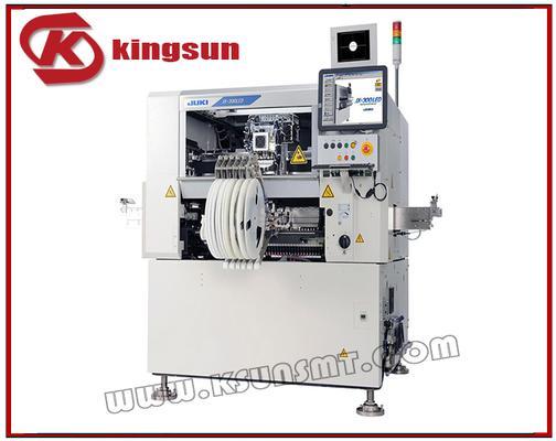
JUKI JX-300 LED SMT Chip Mounter Machine Improvements in Productivity Outstanding Area Productivity Mounting Quality that Supports High Density Mounting Model Interchangeability Model FX-3 FX-1R(Conventional model kind) P
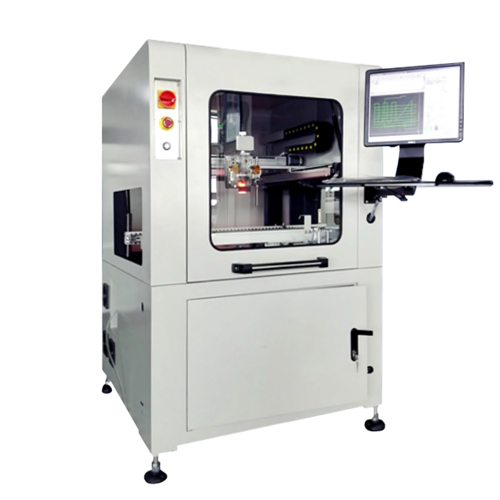
Automatic online glue dispenser HMH830D 1. X, Y, Z three-axis motion, accurately realize the selective spraying process of various circuit boards to avoid non-coated areas such as connectors. 2. Accurately realize the selective area spraying of vari
Electronics Forum | Mon May 23 08:22:31 EDT 2005 | davef
Thermal mass is the ability of a material to absorb heat energy. * A lot of heat energy is required to change the temperature of high density areas, like a ground plane. They are therefore said to have high thermal mass. * Light weight areas, such as
Electronics Forum | Fri Jan 18 18:19:38 EST 2008 | arun2382
Is normal DI rinse cycle enough to wash away all residue after SMT assembly of high density substrate? This substrate would later be over molded to form MCM module package and I am seeing delamination in high density areas of the substrate at MSL3
Used SMT Equipment | Screen Printers
In a good condition! DEK’s Horizon platforms offer a comprehensive array of sophisticated features as standard, including optimised printer frame technology, fast product changeover, 2 Cpk print process capability and 6-sigma production performance.
Used SMT Equipment | Soldering - Reflow
Gently used, high quality, Swiss made Essemtec RO-06-PLUS IR/Convection Drawer-type batch reflow oven. Used machines from Essemtec are difficult to obtain on the market, this is a great opportunity to get one for a good deal! Prototyping / light pr
Industry News | 2003-06-25 12:40:26.0
to manufacture and market printed circuit boards utilizing PCB Channel Routing technology from Nortel Networks
Industry News | 2003-04-14 08:50:52.0
Providing connection facilities for PCBs designed to be used in hazardous areas is straightforward with Phoenix Contact's new range of Combicon Ex-approved printed circuit terminal blocks.
Parts & Supplies | Pick and Place/Feeders
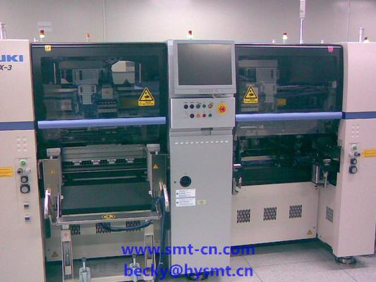
Starting in May 2008, JUKI Corporation (President Kazuyuki Nakamura; listed on First Section of the Tokyo Stock Exchange) is beginning worldwide sales of its High-speed Modular Mounter FX-3. The FX3 is an industrial robot for mounting electronic comp
Technical Library | 2023-01-17 17:58:36.0
Heterogeneous integration has become an important performance enabler as high-performance computing (HPC) demands continue to rise. The focus to enable heterogeneous integration scaling is to push interconnect density limit with increased bandwidth and improved power efficiency. Many different advanced packaging architectures have been deployed to increase I/O wire / area density for higher data bandwidth requirements, and to enable more effective die disaggregation. Embedded Multi-die Interconnect Bridge (EMIB) technology is an advanced, cost-effective approach to in-package high density interconnect of heterogeneous chips, providing high density I/O, and controlled electrical interconnect paths between multiple dice in a package. In emerging architectures, it is required to scale down the EMIB die bump pitch in order to further increase the die-to-die (D2D) communication bandwidth. Aa a result, bump pitch scaling poses significant challenges in the plated solder bump reflow process, e.g., bump height / coplanarity control, solder wicking control, and bump void control. It's crucial to ensure a high-quality solder bump reflow process to meet the final product reliability requirements. In this paper, a combined formic acid based fluxless and vacuum assisted reflow process is developed for fine pitch plated solder bumping application. A high-volume production (HVM) ready tool has been developed for this process.
Technical Library | 2019-10-21 09:58:50.0
An ACI Technologies customer inquired regarding printed circuit board(PCB) failures that were becoming increasingly prevalent after the SMT (surface mount technology) manufacturing process. The failures were detected by electrical testing, but were undetermined as to the location and specific devices causing the failures. The failures were suspected to be caused predominately in the BGA (ball grid array) devices located on specific sites on this 16 layer construction. Information that was provided on the nature of the failures (i.e., opens or shorts) included high resistance shorts that were occurring in those specified areas. The surface finish was a eutectic HASL (hot air solder leveling) and the solder paste used was a water soluble Sn/Pb(tin/lead).
Hear what attendees had to say about the Electronics in Harsh Environments Conference. Start planning your participation for the 2020 event: 21-23 April 2020 | Amsterdam, Netherlands https://www.smta.org/harsh
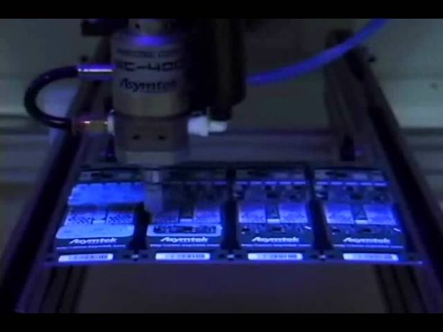
PV inverters require reliability against ingress humidity and dust in harsh environments, like deserts. Conformal coating is critical to protect inverter PCBA. Shown with the SC-400. http://www.nordsonasymtek.com
Training Courses | | | PCB Design Courses
The PCB design courses teach students the process, techniques and tools needed to design layout of printed circuit boards.
Training Courses | | | PCB Rework and Hand Soldering Courses
The PCB rework and hand soldering courses courses cover techniques of rework and repair of PCBs, BGAs and other electronics assemblies, and teach fundamentals of soldering of electronics assemblies.
Events Calendar | Tue Feb 19 00:00:00 EST 2019 - Tue Feb 19 00:00:00 EST 2019 | Elkridge, Maryland USA
SMTA Capital Chapter: Non-Destructive BGA/Area Array Component Rework
Events Calendar | Tue Apr 21 00:00:00 EDT 2020 - Thu Apr 23 00:00:00 EDT 2020 | Amsterdam, Netherlands
Electronics in Harsh Environments Conference
Career Center | Fremont, California USA | Engineering
Job Description: • Has full ownership of HW design and release including HW specification creation, schematic generation, PCB layout, board bring up, and design verification. • Complete PCB design schematic using Orcad capture. • Complete HW desig
Career Center | Melbourne, Florida USA | Engineering,Production
Mechanical Engineer Candidate will work in the Advanced Manufacturing Technology organization executing the development, qualification, and implementation of leading-edge manufacturing processes across a broad range of applications and support manufa
Career Center | Erode, Tamilnadu India | Engineering
Professional Summary 3+ years of experience in the PCB CAM engineering Exposure to FRONTLINE GENESIS 2000 Having exposure in UCAM Exposure to Create, Array & Panelize it for manufacturability Experienced in Creating impedance cou
Career Center | , District of Columbia | Engineering,Management,Production,Sales/Marketing
• Strong technical leadership and decision-making skills; strong verbal and written communication skills to provide clear, crisp direction for key issue resolution; and good team skills to facilitate cross-functional cross -site team effectiveness.
SMTnet Express, November 3, 2016, Subscribers: 26,550, Companies: 15,009, Users: 41,360 A Novel Method for the Fabrication of a High-Density Carbon Nanotube Microelectrode Array Adam Khalifa, Zhaoli Gao, Amine Bermak, Yi Wang, Leanne Lai Hang Chan
| http://etasmt.com/cc?ID=te_news_industry,23961&url=_print
High Speed High Density Open Pin Field Array, has up to 500 I/O contact pins with a solder charge termination. This type of connector looks like a standard BGA type of SMT device
PCB Libraries, Inc. | https://www.pcblibraries.com/forum/footprints-for-high-vibration-and-shock_topic2568_post10485.html
: San Diego, CA Status: Offline Points: 5131 Post Options Post Reply Quote Tom H Report Post Thanks(0) Quote Reply Posted: 06 Nov 2019 at 7:03am Originally, the IPC-7351 Most Density was the solution for high shock and vibration, but 8 years ago the Japanese did tests on the Nominal and Most Density Levels and discovered that there was no