Industry Directory | Manufacturer
Manufacturer of Laser Cut & Chemical Etched Stencils.
Industry Directory | Consultant / Service Provider / Manufacturer
One of the major suppliers of stencils and pallets to the SMT industry. Stentech offers Electroformed and laser cut stencils, pallets and fixtures.
New Equipment | Solder Paste Stencils
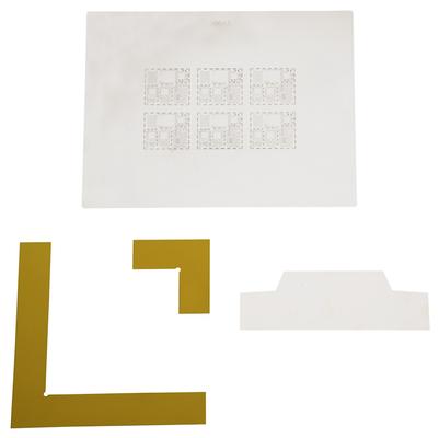
SMT Foil Stencils are laser cut solder paste stencils designed to work on their own for hand printing or with stencil tensioning systems. These laser cut stencils do not need to be permanently glued in a frame. These so-called frameless stencils are

Do you have issues with the height of your paste deposit when printing close to your clamp foils? Let SigmaPrint take you to the EDGE of your printing boundaries! The CustomFoil � (PAT APP FOR) board clamp replacement system from SigmaPrint Technolog
Electronics Forum | Wed Apr 24 21:34:01 EDT 2002 | davef
Search the fine SMTnet Archives. Guidelines * Control: Flux specific gravity, preheater temp, conveyer speed, solder temperature. * Two most important parameters are: solder temperature & dwell time * Contact time. The optimum contact (dwell) time
Electronics Forum | Thu May 18 10:20:55 EDT 2006 | slthomas
Russ asks good questions and I think Chunks pretty much nailed it. Aspect ratio (aperture width/stencil thickness) s/b 1.2 minimum (I like 1.5 if I can get it). If your aperture width = lead width (.008"), yours is 1. Tough to get consistent paste r
Industry News | 2016-02-27 20:41:52.0
BEST Inc. instructors will be conducting 2 training sessions this year at the APEX Expo 2016 - Advanced Rework: Hands-on BGA Reballing, Lead-Free Devices, and Fine-Pitch Parts, and the 2nd session - Stencil Printing: Consistent Print Volumes for SMT Rework.
Industry News | 2015-12-10 17:59:21.0
Metal Etch Services has more than 25 years experience manufacturing High Quality SMT Stencils, based on this experience we offer free technical assistance to all our customers.
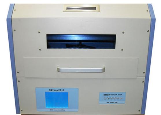
Parts & Supplies | Soldering - Reflow
Brand New SMT2010 TABLE-TOP REFLOW OVEN LEAD-FREE Description: This is a brand new, SMT2010 Reflow oven. More and more surface mount devices (SMD) are used on electronic circuit boards. Large floor model reflow ovens are expensive and heavy, no
Technical Library | 2015-08-25 13:51:27.0
The stencil printing process is one of the most critical processes in the electronic production. Due to the requirement: "faster and smaller" it is necessary to place components with different paste volume close together without regard to solder paste printing. In our days it is no longer possible to control the solder paste volume only by adjustment of the aperture dimensions. The requirements of solder paste volumes for specific components are realized by different thicknesses of metal sheets in one stencil with so called step stencils. The step-down stencil is required when it is desirable to print fine-pitch devices using a thinner stencil foil, but print other devices using a thicker stencil foil. The paper presents the innovative technology of step-up and step-down stencils in a laser cutting and laser welding process. The step-up/step-down stencil is a special development for the adjustment of solder paste quantity, fulfilling the needs of placement and soldering. This includes the laser cutting and laser welding process as well as the resulting stencil characteristics and the potential of the printing process.
Technical Library | 2020-09-02 22:14:36.0
The demand for miniaturization and higher density electronic products has continued steadily for years, and this trend is expected to continue, according to various semiconductor technology and applications roadmaps. The printed circuit board (PCB) must support this trend as the central interconnection of the system. There are several options for fine line circuitry. A typical fine line circuit PCB product using copper foil technology, such as the modified semi-additive process (mSAP), uses a thin base copper layer made by pre-etching. The ultrathin copper foil process (SAP with ultrathin copper foil) is facing a technology limit for the miniaturization due to copper roughness and thickness control. The SAP process using sputtered copper is a solution, but the sputtering process is expensive and has issues with via plating. SAP using electroless copper deposition is another solution, but the process involved is challenged to achieve adequate adhesion and insulation between fine-pitch circuitries. A novel catalyst system--liquid metal ink (LMI)--has been developed that avoids these concerns and promotes a very controlled copper thickness over the substrate, targeting next generation high density interconnect (HDI) to wafer-level packaging substrates and enabling 5-micron level feature sizes. This novel catalyst has a unique feature, high density, and atomic-level deposition. Whereas conventional tin-palladium catalyst systems provide sporadic coverage over the substrate surface, the deposited catalyst covers the entire substrate surface. As a result, the catalyst enables improved uniformity of the copper deposition starting from the initial stage while providing higher adhesion and higher insulation resistance compared to the traditional catalysts used in SAP processes. This article discusses this new catalyst process, which both proposes a typical SAP process using the new catalyst and demonstrates the reliability improvements through a comparison between a new SAP PCB process and a conventional SAP PCB process.
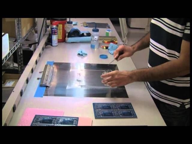
This is video shows how to print a PCB using a prototype foil only stencil. The SMT prototype stencil (www.soldertools.net) is made from a high nickel content material able to offer repeatable high precision apertures. The steps of alignment, printin
This is video shows how to print a PCB using a prototype foil only stencil. The SMT prototype stencil (www.soldertools.net) is made from a high nickel content material able to offer repeatable high precision apertures. The steps of alignment, printin
Training Courses | | | PCB Design Courses
The PCB design courses teach students the process, techniques and tools needed to design layout of printed circuit boards.
foils laminated to polyimide (PI) as flexible pri
KD Electronics Ltd. | http://www.kundasmt.com/?A-Equipment-Accessories/6010.html
FEEDER locking device 30/2 slots 03081674-01 GUIDE PROFILE L=150mm 03081718S01 conversion board cpl. 03081876S02 tamp wheel cpl. Z=44 X16 N 03081908S02 deflector rocker X12/X16 V2 03081927-01 Montageschluessel Imbus Kopfkameras 03081962-01 Cable splice sensor X12/X16 V2 03081975-02 Centering bar 60/2 slots 03081997S02 flap foil disposal X12 V2 cpl
| https://www.eptac.com/wp-content/uploads/2013/09/eptac_09_18_13.pdf