Industry Directory | Manufacturer
Shuttle Star Technology designs and builds advanced off-line 2.5D&3D x-ray inspection systems for solder joint and final assembly test inspection in SMT&EMS. It uses world-class X-ray techniques with advanced defect detection.
Industry Directory | Manufacturer
Manufacturer of materials for the electronics assembly marketplace. Our RoHS-compliant products include solder pastes, fluxes, solder powder, core wire and bar solder and process support products.
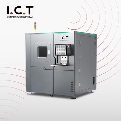
Inline 3D PCB Automated X-ray Inspection System - Advanced Quality Assurance Solution ❙ Introduce of SMT PCBA X-ray Machine Explore our Inline 3D PCB Automated X-ray Inspection System, a cutting-edge solution for advanced quality assurance in PCB
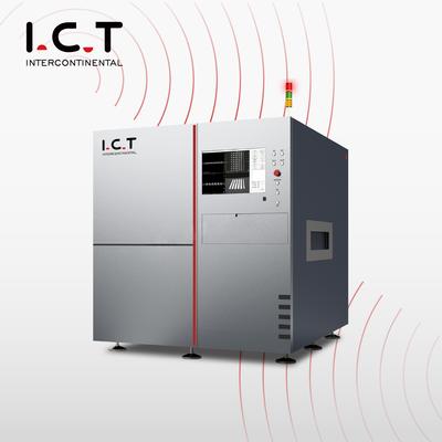
Off-line 3D SMT X-ray Inspection Machine - High-precision Quality Control ❙ Introduce of SMT PCBA X-ray Machine Looking for an off-line 3D SMT X-ray inspection machine? Our high-precision 3D SMT X-ray machine ensures top-notch quality control for
Electronics Forum | Thu Jan 02 22:09:15 EST 2020 | Zack
Hello, Can you give more detail on LGA parts in question? is 50 mm x 50 mm is overall size of the parts? What about pad pitch and how big is the pads individually? I assume that 50x50 mm is overall size. How about the stencil opening for the LGA pad
Electronics Forum | Thu Jun 10 16:42:11 EDT 2010 | daxman
Hi Muarty, We've had a lot of experience with QFN's now. Several years ago we started testing various design methods of the via arrays as well as paste apertures to cover the arrays. There has been some time that has passed now since these packages

Used SMT Equipment | X-Ray Inspection
CR Technology Model Number: CRX2000 Serial Number: 1S1878.0100 Year 2000-2001 Hamamatsu Tube Type -130kV X-Y-Z indexing table with joystick control 18" x 24" X-Y travel Full 360 degrees rotation and tilt up to 90 degrees BGA / Flip Chip Sold
Used SMT Equipment | X-Ray Inspection
we are looking for wth following options: Automatic microfocus X-ray inspection system including: - 160 kV proprietary microfocus X-ray source (open design) with “unlimited” lifetime, including demountable collimator for enhanced image qualit
Industry News | 2016-01-17 19:26:58.0
In order to keep up with industry demand, IPC has released amendments for J-STD-001F, Requirements for Soldered Electrical and Electronic Assemblies, and IPC-A-610F, Acceptability of Electronic Assemblies. For each standard, IPC-A-610F Amendment 1 and IPC J-STD-001F Amendment 1 represents a critical shift to deliver necessary updates to these already robust standards.
Industry News | 2012-02-07 01:05:27.0
The SMTA is pleased to announce the Best Papers from SMTA International 2011. As speakers at SMTA International, individuals make contributions to the industry by sharing their research and findings. To reward exceptional achievement, $1,000 awards and plaques are given for the Best of Conference Presentation, Best of Proceedings Paper, and the Best International Paper.
Technical Library | 2023-01-17 17:22:28.0
The impact of voiding on the solder joint integrity of ball grid arrays (BGAs)/chip scale packages (CSPs) can be a topic of lengthy and energetic discussion. Detailed industry investigations have shown that voids have little effect on solder joint integrity unless they fall into specific location/geometry configurations. These investigations have focused on thermal cycle testing at 0°C-100°C, which is typically used to evaluate commercial electronic products. This paper documents an investigation to determine the impact of voids in BGA and CSP components using thermal cycle testing (-55°C to +125°C) in accordance with the IPC- 9701 specification for tin/lead solder alloys. This temperature range is more typical of military and other high performance product use environments. A proposed BGA void requirement revision for the IPC-JSTD-001 specification will be extracted from the results analysis.
Technical Library | 2020-11-09 16:59:53.0
A customer contacted ACI Technologies regarding a high failure rate of their assemblies. They provided assemblies to be X-rayed and inspected for the purpose of identifying any process related issues such as (but not limited to) solder and assembly workmanship and evidence of damage due to moisture related problems during reflow (a.k.a. "popcorning"). Moisture damage usually appears as physical damage to the component. The first indication of moisture damage would be externally observable changes to the package in the form of bulging or fractures to the outer surface of the component, an example of which is shown in Figure 1. Internally observable indicators of moisture damage typically include fractures to the die inside the package and lifted or fractured wire bonds. These conditions would be apparent during transmissive X-ray inspection. Another symptom of moisture related damage would be inconsistent solder joint sizes that result from package deformation during the liquidus phase of the reflow process. None of these indicators of moisture related damage were present on the customer samples.

· What is the difference between SMT vacuum reflow soldering machine and ordinary reflow soldering machine? · What problems can be solved by smt vacuum reflow soldering machine? · What is the basic principle of vacuum reflow machine? · Ho

ACI Technologies Inc. (ACI) is a scientific research corporation dedicated to the advancement of electronics manufacturing processes and materials for The Department of Defense and industry. This video provides an overview of our commercial service
Training Courses | | | PCB Rework and Hand Soldering Courses
The PCB rework and hand soldering courses courses cover techniques of rework and repair of PCBs, BGAs and other electronics assemblies, and teach fundamentals of soldering of electronics assemblies.
Training Courses | | | PCB Rework and Hand Soldering Courses
The PCB rework and hand soldering courses courses cover techniques of rework and repair of PCBs, BGAs and other electronics assemblies, and teach fundamentals of soldering of electronics assemblies.
Events Calendar | Tue Feb 12 00:00:00 EST 2019 - Tue Feb 12 00:00:00 EST 2019 | ,
Webinar: BGA and Area Array Process Defects - Causes & Cures
Events Calendar | Mon Mar 16 00:00:00 EDT 2020 - Mon Mar 16 00:00:00 EDT 2020 | ,
BGA & Area Array Failures, Causes & Corrective Actions Online Webinar
SMTnet Express, October 10, 2019, Subscribers: 32,263, Companies: 10,893, Users: 25,93 Fill the Void IV: Elimination of Inter-Via Voiding Credits: FCT ASSEMBLY, INC. Voids are a plague to our electronics and must be eliminated! Over the last few
SMTnet Express, October 3, 2018, Subscribers: 31,373, Companies: 11,056, Users: 25,258 Fill the Void II: An Investigation into Methods of Reducing Voiding Tony Lentz - FCT Assembly , Patty Chonis, JB Byers - A-Tek Systems Voids in solder joints
| https://www.eptac.com/faqs/ask-helena-leo/ask/problems-with-pcb-micro-voiding
Problems With PCB Micro Voiding - EPTAC - Train. Work Smarter. Succeed Looking for solder training standards, manuals, kits, and more
Heller 公司 | http://hellerindustries.com.cn/Vacuum-Void-Reduction-Reflow.pdf
processing. Cross sectional views of the voiding are shown in the optical photomicrographs in Figure 9. Many of the voids observed in the cross-sectional analysis exceed the IPC-JSTD-001 BGA maximum void criteria of 30% of the X-ray image area [23]. This

.gif)