
Industry Directory | Consultant / Service Provider / Media / Publisher / Online Resource / Other
PCB Libraries' "Footprint Expert" suite uses CAD LEAP(tm) Technology to greatly simplify footprint and 3D STEP model creation; it is used by tens of thousands of PCB designers and engineers all over the world.
A minority owned business with 40 plus years of experience that can fit your needs, in electrical engineering, printed circuit board, and mechanical design. With Alta Design Corp, we want to be an extension of your company. We understand the meaning of �Time to Market� and will ensure we meet your due date, while being price competitive.
New Equipment | Assembly Services
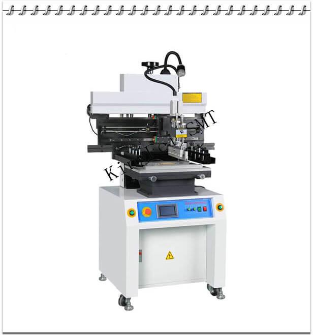
Product features: The servo system is convenient and accurate for positioning. The Japanese THK guide rail and Taiwan STK variable frequency motor are used to drive the scraper base to ensure the printing accuracy. The printing scraper can be rota

technical parameter Model: s1200 (special type for LED light bar) Overall dimension (L × w × h): 1650 × 620 × 1550 (mm) Platform size: 320 × 1300 (mm) PCB size: 250 × 1250 (mm) Applicable template size: 550 ×
Electronics Forum | Fri Jan 06 05:03:11 EST 2012 | richieoreilly
Hi All, Just wondering if anyone is placing 0201 components in volume. If so What pad layout are you using, i.e. pad size, shape and spacing. Also are you pads and fiducials solder mask defined or copper defined. Can you also let me know the rough q
Electronics Forum | Fri Jan 06 13:47:15 EST 2012 | davef
Your starting [and finishing] point should be IPC-7351B Land Pattern Calculator and Tools - http://landpatterns.ipc.org/default.asp For more, look here: * http://www.smtnet.com/bob-willis/pbdai.html * http://www.onboard-technology.com/pdf_novembre

Used SMT Equipment | Pick and Place/Feeders
MC389CY-F3-V MC-389 High-Speed, High-Mix Pick & Place WITH CONVEYOR Heavy-duty, welded steel base frame w/ adjustable foot pads High-precision ball screw X-Y drive mechanism w/ linear encoders Three pick and place heads, each with servo-drive

Used SMT Equipment | Pick and Place/Feeders
Heavy-duty, welded steel base frame w/ adjustable foot pads High-precision ball screw X-Y drive mechanism w/ linear encoders Three pick and place heads, each with servo-driven Z- and ?-axis motors Standard on-the-fly vision alignment cameras for c
Industry News | 2011-09-12 12:04:25.0
GPD Global will showcase its Positive Cavity Displacement (PCD) 'H' Series high-resolution pumps in Booth #439 at the upcoming IMAPS 44th International Symposium on Microelectronics
Industry News | 2011-11-20 13:36:13.0
GPD Global has been awarded two Global Technology Awards in the categories of Adhesives/Coatings/Encapsulants and Dispensing Equipment for its PCD Dispensing on the MAX Series Platform

Parts & Supplies | Assembly Accessories
M001 I-PULSE Nozzle M2 PK NZ -N001 (0.5 X 0.4)mm N002 I-PULSE Nozzle M2 PK NZ -N002 (0.9 X 0.62) N003 I-PULSE Nozzle M2 PK NZ -N003 (1.3 X 0.7) N004 I-PULSE Nozzle M2 PK NZ -N004 (1.8 X 1.2) N005 I-PULSE Nozzle M2 PK
Parts & Supplies | Assembly Accessories
KJK-M1300-000 YAMAHA FSII82 feeder feeder hit 0201 0402 component feeder KJK-M1500-010 000 YG12 feeder YAMAHA FT8x2 FT8 * 2mm feeder KJW-M1200-023 YAMAHA feeder YAMAHA FT84mm feeder YG12 dedicated feeder KJW-M1200-02X KJW-M1200-021 YG12 FT8 * 4
Technical Library | 2020-04-14 15:56:32.0
This paper will focus on the application requirements of solder printing small aperture designs, concentrating on 008004 (inch) / 0201 (metric) size components, and the results of a design of experiment printing these challenging apertures. As Moore's law continues to be applied to component miniaturization, the next installment of reduced packaging has arrived in the form of the 008004/0201 for resistors and capacitors. Component size roughly the size of a grain of sand presents specific challenges to the solder printing process. To address these challenges, each aspect of the printing process will need be examined. This includes essential machine requirements, including correct squeegee blades, tooling support, and calibrations, to meet the demanding specifications. The correct match and design of materials will be addressed, focusing on the stencil and substrate design along with solder paste and cleaning solvent requirements. A design of experiment will be reviewed that applies the machine and materials discussed, including the printer and Solder Paste Inspection (SPI) setup and the specific machine parameters used. The results of these DOE's will then be closely examined.
Technical Library | 2020-05-08 18:22:31.0
A customer contacted the Helpline to perform analysis on a lead-free assembly which exhibited intermittent functionality. The lead-free assembly exhibiting intermittent functionality when pressure was applied to the ball grid array (BGA) packages. Industrial adaptation of a Restriction of Hazardous Substances (RoHS) compliant solder standard has created a new host of failure modes observed in lead-free assemblies. Pad cratering occurs when fractures propagate along the epoxy resin layer on the underside of the BGA connecting pads. While originating from process, design, and end use conditions, it is the combination of a rigid lead-free solder with inflexible printed circuit board (PCB) laminates that has advanced the prevalence of this condition. Pad cratering is simply the result of mechanical stress exceeding material limitations.

www.unisoft-cim.com/pcbtest.htm - In minutes the Unisoft ProntoTEST-FIXTURE software translates CAD & BOM files into real reference designators, netlists, X/Y component pin geometries, values, tolerances, part numbers, etc. This data is used by Test

The PCB Footprint Expert is a powerful CAD library development tool powered by our own proprietary CAD LEAP Technology (Libraries Enhanced with Automated Preferences). It is packed with very powerful advanced library management features that cuts foo
Training Courses | | | PCB Rework and Hand Soldering Courses
The PCB rework and hand soldering courses courses cover techniques of rework and repair of PCBs, BGAs and other electronics assemblies, and teach fundamentals of soldering of electronics assemblies.
Training Courses | | | PCB Rework and Hand Soldering Courses
The PCB rework and hand soldering courses courses cover techniques of rework and repair of PCBs, BGAs and other electronics assemblies, and teach fundamentals of soldering of electronics assemblies.
Events Calendar | Wed May 31 00:00:00 EDT 2023 - Wed May 31 00:00:00 EDT 2023 | Holtsville, New York USA
Long Island Chapter Meeting: Fine Feature Paste Printing, Stencil Design and Solder Technology
Events Calendar | Thu Mar 18 00:00:00 EDT 2021 - Thu Mar 18 00:00:00 EDT 2021 | ,
India Chapter Webinar: PCBA Process Qualifications
Career Center | Sherman, Texas USA | Engineering,Production,Research and Development,Technical Support
SMT Packaging Engineer: Location: Texas - Sherman , TX Group: HVAL Degree Requirements: BS ME/ChemE/Materials The person in this position will have the ability to make very significant financial contributions to TI because this is a very critic
Career Center | Lincoln, Nebraska USA | Engineering
Brief Description of Job Duties: Provide new program engineering support with emphasis on technical SMT process development. Key activities would include recommendations and implementation of components, SMT pad design, solder methods, testing and r
Career Center | Bangalore, India | Engineering,Maintenance,Production,Technical Support
SMT Stencil designing & Knowledge of full SMT process software known CAD/CAM -circuit CAM Pro 7.3,GC Power station, GCCAM Edit,Auto CAD, Fault finding of Electronic Boards & Servicing electronic machines.
Career Center | Newport Beach, California USA | Engineering,Management,Production
KEVIN RAGER P.O.BOX 7878, NEWPORT BEACH, 949 922 8997, KEVIN.RAGER@EDA-INC.US OBJECTIVE I am trying to find a consistent work flow that provides mentally challenging yet stimulating experiences in design and prototype development. EXPERIENCE 1997
PCB Libraries, Inc. | https://www.pcblibraries.com/forum/design-smt-pad-for-magnet-wire_topic1206.html
Design SMT pad for magnet wire - PCB Libraries Forum Forum Home > PCB Footprint Expert > Questions & Answers New Posts FAQ Search Events Register Login Design SMT pad for magnet wire
Imagineering, Inc. | https://www.pcbnet.com/blog/considerations-for-pcb-board-design-layout/
Considerations for PCB Board Design & Layout | Imagineering, Inc. Skip to main content Resources Support Contact Us FAQs Live Chat My Account 847-806-0003 Menu PCB Capabilities Fabrication Technology Roadmap Materials Available HDI Tolerances Certifications


