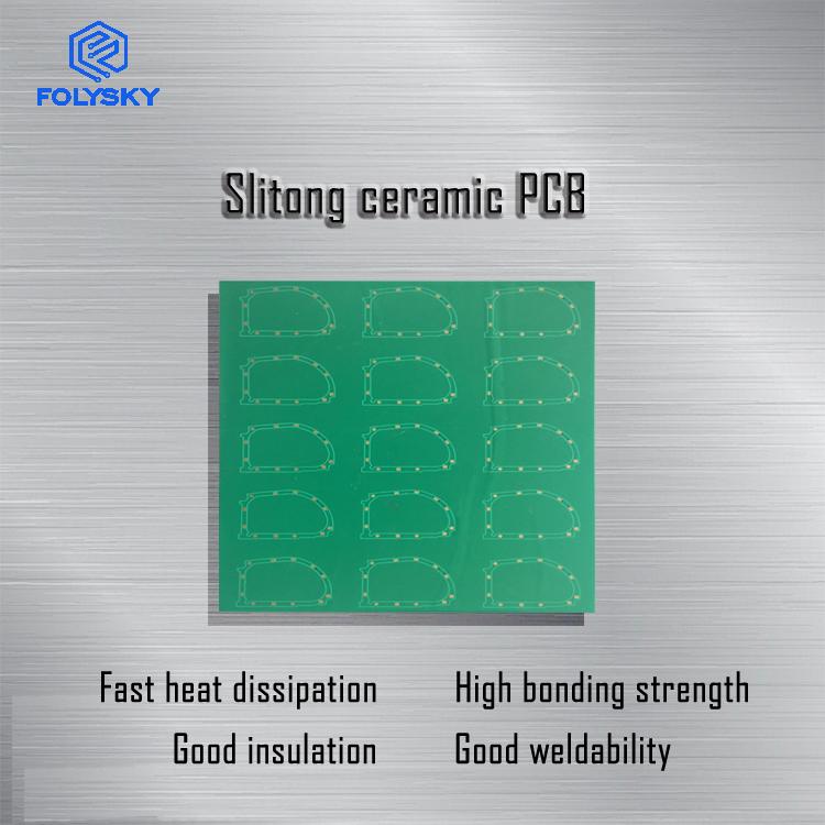
与PCB标称,Sliton陶瓷产品具有耐压性、可更换性和电子照明性、智能芯片、材料、航空航天、LED、传感器等领域和金属化技术,具有速度快、交货快快捷、尺寸选择、规格和定制等优点。 基础类型:工业生产 材料研究进展:0.5毫米 导电层:铜 金属层厚度:35μm的/35μm的 表面处理:重银 金属单面/双面:双面 镀铜通孔:是的 焊锡面膜:是的
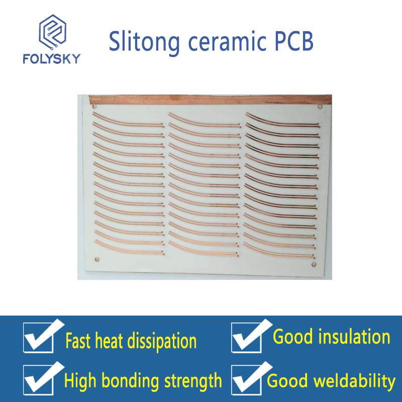
LED,LED封装厂在发布用于于的的的的,cob支架,cob支架,cob一些潜在,cob支架支架的加工加工与与传统传统的的的的的的的的的的的的的的的并正向5W发展。 基础类型:工业生产 材料加工厚度:0.38mm 导电层:铜 金属层厚度:100μm/35μm 表面处理:浸金 金属单面/双面:双面 镀铜通孔:是的 焊锡面膜:是的
在我们的专业团队的帮助下,我们的最小光圈值可以达到0.06 mm,线宽和距离的偏移可以达到0.1 mm以下,而行业的光圈可能为0.15-0.5mm。3D陶瓷板,因为传统工业通常采用图形电镀或直接蚀刻来制作电路,这些但是,我们的LAM技术可以选择镀铜并直接制作电路, 基材类型:氧化铝陶瓷 基板材料厚度:0.65mm 导电层:铜 金属层厚度:200μm 表面处理:OSP 金属单面/双面:双面 镀铜通孔:是的 焊锡面膜:是的
Petroferm has the solution for removal of post reflow residues from every available solder paste and flux. Petroferm offers a complete line of aqueous, semi-aqueous, and solvent defluxing chemistries for use in every brand and style of cleaning equip
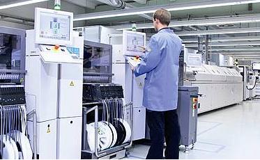
9 SMT Assembly Lines Total placement capability 150,000 components/hr Fine pitch placement up to 12mil Component Ranges: 0201 to BGA and uBGA up to 55mm square 40 microns placement accuracy with 4 sigma capability RoHS Compliant Lines with N2 envi
Eclipse Industries DS-107 Aligner Bonder The DS-107 Aligner Bonder is an ultra-high precision, high or low force aligner bonder. Constructed on a granite platform for superior stability and rigidity, the DS-107 is designed for alignment accuracy of
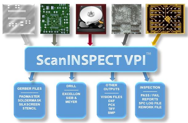
ScanINSPECT VPI is a fully integrated, stand-alone process control, measurement and inspection and programming workstation for use in process setup and new product introduction in the PCB or Hybrid Microcircuit assembly industries. ScanINSPECT VPI
Lite Fast SR-1000, a UV Solder Mask, was designed to screen print over conductive traces, landing pads, resistors, fuses and capacitors on Printed Circuit Boards (PCBs) and ceramic substrates. Other applications include metal and various plastics.
New Equipment | Assembly Services
Benefit from our versatility and experience. We manufacture rigid printed circuit boards, rigid-flex and flexible printed circuit boards [including crimp technology]. You`ll find us flexible as far as dimensions are concerned: in addition to standard