Industry News | 2012-10-17 11:24:10.0
Nihon Superior Co., Ltd. announces that it was awarded a 2012 Global Technology Award in the category of Materials – Solder Paste for its SN100C P810 D4 No-Clean Lead-Free Solder Paste.
Industry News | 2009-11-19 14:48:22.0
Broadening its well-known Multicore die attach solder portfolio, which already includes Multicore DA100 solder paste for high-lead and lead-free applications, Henkel today announced the launch of Multicore DA101. This newest formulation delivers many of the well-known benefits of Multicore DA100, but has been designed for screen print operations, thus offering flexibility for varying process requirements.
Industry News | 2009-07-24 13:38:04.0
To address the thermal requirements posed by smaller outline, higher functioning power semiconductor devices, Henkel has formulated an advanced die attach solder paste suitable for both high-lead and lead-free applications.
Technical Library | 2020-07-15 18:29:34.0
In the early 2000s the first fine-pitch ball grid array devices became popular with designers looking to pack as much horsepower into as small a space as possible. "Smaller is better" became the rule and with that the mechanical drilling world became severely impacted by available drill bit sizes, aspect ratios, and plating methodologies. First of all, the diameter of the drill needed to be in the 0.006" or smaller range due to the reduction of pad size and spacing pitch. Secondly, the aspect ratio (depth to diameter) became limited by drill flute length, positional accuracy, rigidity of the tools (to prevent breakage), and the throwing power of acid copper plating systems. And lastly, the plating needed to close up the hole as much as possible, which led to problems with voiding, incomplete fill, and gas/solution entrapment.
Industry News | 2022-01-10 16:39:30.0
Indium Corporation's Ron Lasky, Ph.D., PE, senior technologist, will share his industry knowledge and expertise during two presentations at the SMTA Pan Pacific Microelectronics Symposium (SMTA PanPac), Jan. 31-Feb. 3, Honolulu, O'ahu, Hawaii, U.S.
Industry News | 2012-07-10 11:27:53.0
Nihon Superior (Singapore) Pte. Ltd.,announces that it will showcase a new, expanded range of products in booth G2 at the upcoming IPCA INTERNATIONAL EXPO 2012, scheduled to take place July 25-27, 2012 in KTPO TRADE CENTRE, WHITEFIELD, in BANGALORE, INDIA.
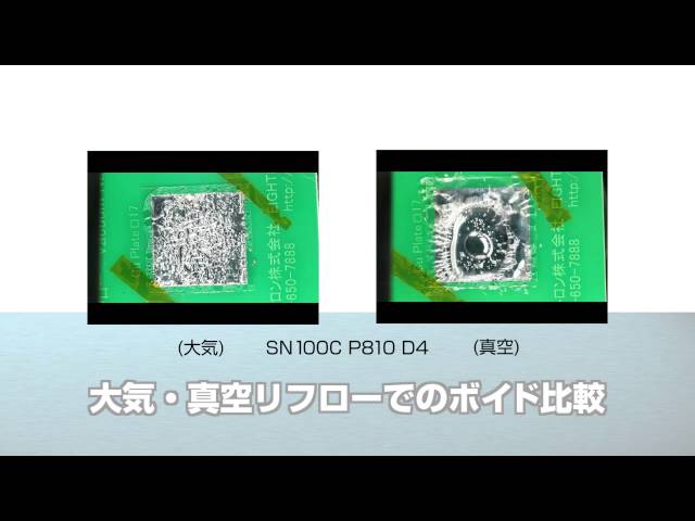
SN100C P810 D4????????? ???????????? ??????????????????????????????????? ?????????????? ???http://www.nihonsuperior.co.jp/
Technical Library | 2019-05-01 23:18:27.0
Moisture can accelerate various failure mechanisms in printed circuit board assemblies. Moisture can be initially present in the epoxy glass prepreg, absorbed during the wet processes in printed circuit board manufacturing, or diffuse into the printed circuit board during storage. Moisture can reside in the resin, resin/glass interfaces, and micro-cracks or voids due to defects. Higher reflow temperatures associated with lead-free processing increase the vapor pressure, which can lead to higher amounts of moisture uptake compared to eutectic tin-lead reflow processes. In addition to cohesive or adhesive failures within the printed circuit board that lead to cracking and delamination, moisture can also lead to the creation of low impedance paths due to metal migration, interfacial degradation resulting in conductive filament formation, and changes in dimensional stability. Studies have shown that moisture can also reduce the glass-transition temperature and increase the dielectric constant, leading to a reduction in circuit switching speeds and an increase in propagation delay times. This paper provides an overview of printed circuit board fabrication, followed by a brief discussion of moisture diffusion processes, governing models, and dependent variables. We then present guidelines for printed circuit board handling and storage during various stages of production and fabrication so as to mitigate moisture-induced failures.
Technical Library | 2019-06-20 00:09:49.0
It is well known that during service the layer of Cu6Sn5 intermetallic at the interface between the solder and a Cu substrate grows but the usual concern has been that if this layer gets too thick it will be the brittleness of this intermetallic that will compromise the reliability of the joint, particularly in impact loading. There is another level of concern when the Cu-rich Cu3Sn phase starts to develop at the Cu6Sn5/Cu interface and an imbalance in the diffusion of atomic species, Sn and Cu, across that interface results in the formation at the Cu3Sn/Cu interface of Kirkendall voids, which can also compromise reliability in impact loading. However, when, as is the case in some microelectronics, the copper substrate is thin in relation to the volume of solder in the joint an overriding concern is that all of the Cu will be consumed by reaction with Sn to form these intermetallics.This paper reports an investigation into the kinetics of the growth of the interfacial intermetallic, and the consequent reduction in the thickness of the Cu substrate in solder joints made with three alloys, Sn-3.0Ag-0.5Cu, Sn-0.7Cu-0.05Ni and Sn-1.5Bi-0.7Cu-0.05Ni.
Technical Library | 2023-11-20 18:10:20.0
The electronics production is prone to a multitude of possible failures along the production process. Therefore, the manufacturing process of surface-mounted electronics devices (SMD) includes visual quality inspection processes for defect detection. The detection of certain error patterns like solder voids and head in pillow defects require radioscopic inspection. These high-end inspection machines, like the X-ray inspection, rely on static checking routines, programmed manually by the expert user of the machine, to verify the quality. The utilization of the implicit knowledge of domain expert(s), based on soldering guidelines, allows the evaluation of the quality. The distinctive dependence on the individual qualification significantly influences false call rates of the inbuilt computer vision routines. In this contribution, we present a novel framework for the automatic solder joint classification based on Convolutional Neural Networks (CNN), flexibly reclassifying insufficient X-ray inspection results. We utilize existing deep learning network architectures for a region of interest detection on 2D grayscale images. The comparison with product-related meta-data ensures the presence of relevant areas and results in a subsequent classification based on a CNN. Subsequent data augmentation ensures sufficient input features. The results indicate a significant reduction of the false call rate compared to commercial X-ray machines, combined with reduced product-related optimization iterations.