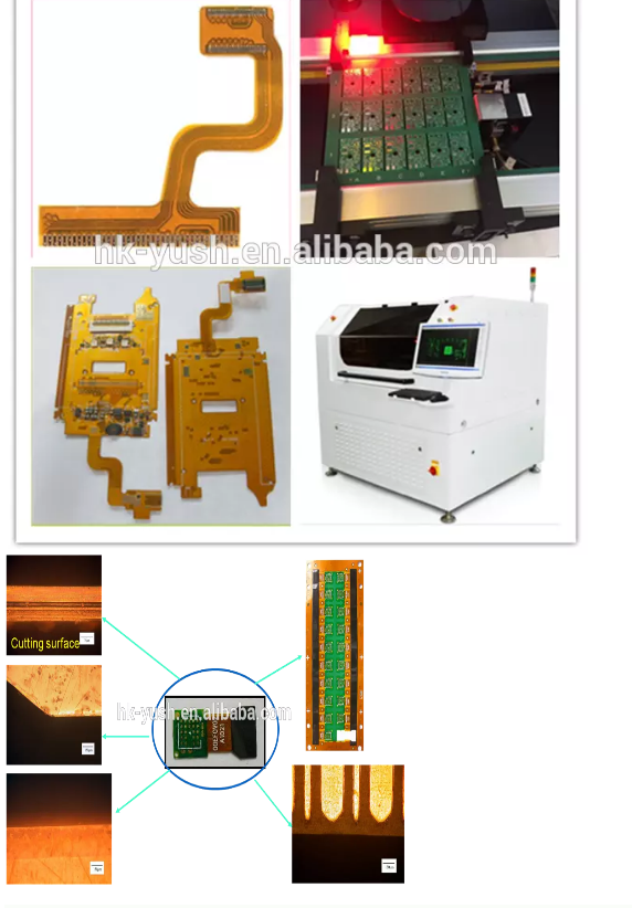
Inline Laser Cutting Machine for Flexible Circuit Boards without Stress Cutting Application FPC and some relative materials; FPC/PCB/ Rigid-Flex PCB cutting, Camera module cutting Features More quick and easy, shorten the de
Industry Directory | Manufacturer
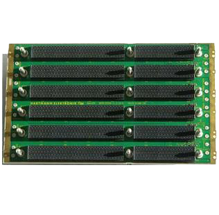
1-20 layers PCB manufacturer, focusing on metal core pcb, multi-layer PCB, fast PCB and middle-small batch PCB. Min. circuit width & spacing: 3mil. UL, ISO9001, ROHS,ISO14001 certified.
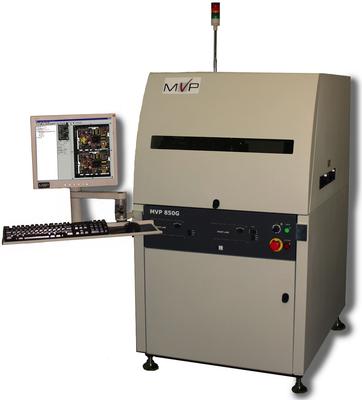
Microelectronics and Semiconductor Inspection. MVP's 850G provides the highest accuracy flip-chip, die assembly inspection. Ensuring the correct placement of the die on the substrate, while providing edge, FM and surface inspection. The 850G modu
Technical Library | 2021-11-03 17:05:39.0
Additively printed circuits provide advantages in reduced waste, rapid prototyping, and versatile flexible substrate choices relative to conventional circuit printing. Copper (Cu) based inks along with intense pulsed light (IPL) sintering can be used in additive circuit printing. However, IPL sintered Cu typically suffer from poor solderability due to high roughness and porosity. To address this, hybrid Cu ink which consists of Cu precursor/nanoparticle was formulated to seed Cu species and fill voids in the sintered structure. Nickel (Ni) electroplating was utilized to further improve surface solderability. Simulations were performed at various electroplating conditions and Cu cathode surface roughness using the multi-physics finite element method. By utilizing a mask during IPL sintering, conductivity was induced in exposed regions; this was utilized to achieve selective Ni-electroplating. Surface morphology and cross section analysis of the electrodes were observed through scanning electron microscopy and a 3D optical profilometer. Energy dispersive X-ray spectroscopy analysis was conducted to investigate changes in surface compositions. ASTM D3359 adhesion testing was performed to examine the adhesion between the electrode and substrate. Solder-electrode shear tests were investigated with a tensile tester to observe the shear strength between solder and electrodes. By utilizing Cu precursors and novel multifaceted approach of IPL sintering, a robust and solderable Ni electroplated conductive Cu printed electrode was achieved.
Technical Library | 2021-11-03 16:49:59.0
Ultrathin bare die chips were soldered using a novel soldering technology. Using homogeneous flash light generated by high-power xenon flash lamp the dummy components and the bare die NFC chips were successfully soldered to copper tracks on polyimide (PI) and polyethylene terephthalate (PET) flex foils by using industry standard Sn-Ag-Cu lead free alloys. Due to the selectivity of light absorption, a limited temperature increase was observed in the PET substrates while the chip and copper tracks were rapidly heated to a temperatures above the solder melting temperature. This allowed to successfully soldered components onto the delicate polyethylene foil substrates using lead-free alloys with liquidus temperatures above 200 °C. It was shown that by preheating components above the decomposition temperature of solder paste flux with a set of short low intensity pulses the processing window could be significantly extended compared to the process with direct illumination of chips with high intensity flash pulse. Furthermore, it was demonstrated that with localized tuning of pulse intensity components having different heat capacity could be simultaneously soldered using a single flash pulse.

Bicheng provides R&D, high-tech, IT research companies and organizations large or small with high frequency RF/microwave PCB's. Technical parameters: *NPTH and PTH( 20 um) *Thermal stress: 288C/10sec *Permitivity: ER2.1-1
New Equipment | Assembly Services
Layers 2-64L Plate Thiickness 0.6-10mm Minimum mechanical aperture 0.2mm Minimum laser aperture 4mil HDI Type 1+n+1、2+n+2、3+n+3 Minimum line width & spacing 4/4mil

New Equipment | Assembly Services
Layers 2-64L Plate Thiickness 0.6-10mm Minimum mechanical aperture 0.2mm Minimum laser aperture 4mil HDI Type 1+n+1、2+n+2、3+n+3 Minimum line width & spacing 4/4mil

New Equipment | Assembly Services
Layers 2-64L Plate Thiickness 0.6-10mm Minimum mechanical aperture 0.2mm Minimum laser aperture 4mil HDI Type 1+n+1、2+n+2、3+n+3 Minimum line width & spacing 4/4mil