客户的计算机电路板是根据客户提供的计算机电路板,是根据客户提供的计算机电路板,来解决生产的问题。电路板。 基础类型:工业生产 材料加工工艺:0.635mm 导电层:Cu,Ni,Au 金属层厚度:300μm 表面处理:浸金 金属单面/双面:单面 镀铜通孔:没有 焊锡面膜:没有

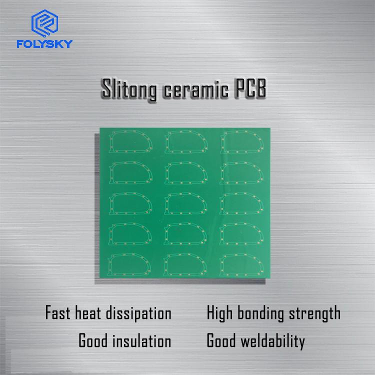
与普通PCB,Sliton陶瓷陶瓷更耐压,可深入智能照明、智能芯片、电子材料、航空航天、LED、传感器等领域。、规格和定制等。 产品名称:其他陶瓷PCB材料厚度:3mm 导电层:Cu 金属层厚度:100μm 表面处理:OSP 金属单面/双面:双面 镀铜通孔:无 阻焊:无

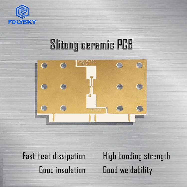
客户订购的陶瓷电路板是根据客户提供的CAD输出,通过客户生产的陶瓷电路板作为一种高热、高介电常数的功能基础,可接入卫星定位、重点医疗、电信产品芯片等,客户要求不同类型和厚度的陶瓷材料可根据特殊加工功能的陶瓷电路板。 名称: 陶瓷金属化 基础厚度:0.65mm 导电层:铜 金属层厚度:200μm 表面处理:OSP 金属单面/双面:双面 镀铜通孔:是 阻焊:有

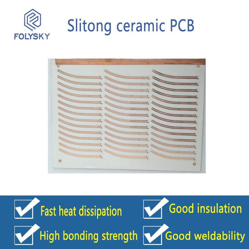
与PCB标称,Sliton陶瓷产品具有耐压性、可更换性和电子照明性、智能芯片、材料、航空航天、LED、传感器等领域和金属化技术,具有速度快、交货快快捷、尺寸选择、规格和定制等优点。 基础类型:工业生产 材料研究进展:0.5毫米 导电层:铜 金属层厚度:35μm的/35μm的 表面处理:重银 金属单面/双面:双面 镀铜通孔:是的 焊锡面膜:是的
LED,LED封装厂在发布用于于的的的的,cob支架,cob支架,cob一些潜在,cob支架支架的加工加工与与传统传统的的的的的的的的的的的的的的的并正向5W发展。 基础类型:工业生产 材料加工厚度:0.38mm 导电层:铜 金属层厚度:100μm/35μm 表面处理:浸金 金属单面/双面:双面 镀铜通孔:是的 焊锡面膜:是的
Industry Directory | Manufacturer
US manufacturer of metallized ceramic substrates & packages; specializing in PCTF (plated copper over thick film) & low cost AgENIG (silver with electroless nickel and immersion gold plating).
在我们的专业团队的帮助下,我们的最小光圈值可以达到0.06 mm,线宽和距离的偏移可以达到0.1 mm以下,而行业的光圈可能为0.15-0.5mm。3D陶瓷板,因为传统工业通常采用图形电镀或直接蚀刻来制作电路,这些但是,我们的LAM技术可以选择镀铜并直接制作电路, 基材类型:氧化铝陶瓷 基板材料厚度:0.65mm 导电层:铜 金属层厚度:200μm 表面处理:OSP 金属单面/双面:双面 镀铜通孔:是的 焊锡面膜:是的
Optical polishing, edge polishing, dicing, flat lapping and machining of all hard materials including ceramic substrates, quartz, AlN, glass and sapphire windows, silicon wafers and very thin substrates and windows.
Industry Directory | Manufacturer
Semiconductor Enclosures Incorporated (SEI) is a powder to package, fully integrated HTCC precision ceramics manufacturer located in Newburyport, Massachusetts. Tape systems, metallization, packages.
Industry Directory | Manufacturer
special machines, loaders, production lines for placing odd shape components, dome foils, mdf, shields, speaker,camera, card reader,screwing, transport, dispencer, singulation and depaneling (punsh units) of ceramic substrats,