May 20, 2023
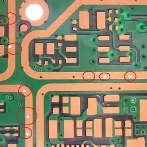
Causes of tin beads
1. Improper setting of the reflow temperature curve. If the temperature in the preheating zone rises too fast, the moisture and solvent inside the solder paste will not be completely volatilized, and the moisture and solvent will boil when it reaches the reflow zone, and the solder paste will splash out to form tin beads.
2. Improper design and structure of steel mesh opening. If solder balls always appear at the same location, it is necessary to check the stencil opening structure. The stencil causes missing printing and unclear printed outlines, bridging each other, and a large number of tin beads will inevitably be generated after reflow soldering.
3. The time between the completion of chip processing and reflow soldering is too long. If the time from placement to reflow soldering is too long, the solder particles in the solder paste will oxidize and deteriorate, and the activity will decrease, which will cause the solder paste not to reflow and produce tin beads.
4. During placement, the z-axis pressure of the placement machine causes the solder paste to be squeezed out of the pad at the moment the component is attached to the PCB, which will also lead to the formation of solder beads after soldering.
5. Insufficient cleaning of PCB boards with solder paste printing errors makes solder paste remain on the surface of the PCB board and in the through holes, which is also the cause of solder balls.
6. During the component mounting process, the solder paste is placed between the chip components’ pins and pads. If the pads and component pins are not well wetted, part of the liquid solder will flow out from the weld, forming Tin beads.
Solution
1. Adjust the reflow soldering temperature curve and strictly control the temperature rise rate in the preheating zone.
2. According to the difference in the shape of the pad, select the appropriate stencil opening mode, and ensure the quality of solder paste printing according to the requirements of the manufacturing process.
3. Selecting a solder paste with a longer use time (at least 4 hours) will reduce this effect. Make sure the solder paste is thawed and stirred before use.
4. Set the parameters of the placement machine, and set different placement heights according to the height of components to ensure that the solder paste on the pad is not squeezed.
5. The sense of responsibility of operators and craftsmen in the production process should be strengthened, production should be strictly followed by the process requirements and operating procedures, and the quality control of the process should be strengthened.
6. Select the appropriate solder paste and pay strict attention to the storage environment of components and PCB.
The above content the reason and solutions for PCBA solder balls is shared by SZTech-SMT for you about the causes and solutions of tin beads in SMT chip processing. I hope it will be helpful to you! To learn more about SMT chip processing, welcome to visit www.sztech-smt.com
.gif)