Nov 05, 2019
8 Layer PCB Stack-up Guidelines
How to improve EMC performance on 8 layer PCB design?
The following text is reproduced, with permission, from Part 4 of a 6-Part article on PCB Stackup by Henry W. Ott. The original article is available at http://www.hottconsultants.com/tips.html
An eight-layer board can be used to add two more routing layers or to improve EMC performance by adding two more planes. Although we see examples of both cases, I would say that the majority of eight layer board stack-ups are used to improve EMC performance rather than add additional routing layers. The percentage increase in cost of an eight-layer board over a six-layer board is less than the percentage increase in going from four to six layers, hence making it easier to justify the cost increase for improved EMC performance. Therefore, most eight-layer boards consist of four wiring layers and four planes.
An eight-layer board provides us, for the first time, the opportunity to easily satisfy all of the five originally stated objectives. Although there are many stack-ups possible, we will only discuss a few of them that have proven themselves by providing excellent EMC performance. As stated above, eight layers is usually used to improve the EMC performance of the board, not to increase the number of routing layers.
An eight-layer board with six routing layers is definitely not recommended, no matter how you decide to stack-up the layers. If you need six routing layers you should be using a ten-layer board. Therefore, an eight-layer board can be thought of as a six-layer board with optimum EMC performance.
The basic stack-up of an eight-layer board with excellent EMC performance is shown in Fig 9.

This configuration satisfies all the objectives listed in my previous post. All signal layers are adjacent to planes, and all the layers are closely coupled together. The high-speed signals are buried between planes, therefore the planes provide shielding to reduce the emissions from these signals. In addition the board uses multiple ground planes, thus decreasing the ground impedance.
For best EMC performance and Signal Integrity, when high frequency signals change layers (e.g., from layer 4 to 5) you should add a ground-to-ground via between the two ground planes, near the signal via, in order to provide an adjacent return path for the current.
The stack-up in Fig. 9 can be further improved by using some form of embedded PCB capacitance technology (e.g. Zycon Buried Capacitanceú) for layers 2-3 and 6-7. This approach provides a significant improvement in the high frequency decoupling and may allow the use of significantly fewer discrete decoupling capacitors.
Another excellent configuration, and one of my favorite, is shown in Figure 10. This configuration includes two outer layer ground planes. With this arrangement all routing layers are buried between planes and are therefore shielded.

H1 indicates the horizontal routing layer for signal 1, and V1 indicates the vertical routing layer for signal 1. H2 and V2 represent the same for signal 2. Although not commonly used this configuration also satisfies all the five objectives presented previously, and has the added advantage of routing orthogonal signals adjacent to the same plane. Typical layer spacing for this configuration might be 0.010"/0.005"/0.005"/0.20"/0.005"/0.005"/0.010"
Another possibility for an eight-layer board is to modify Fig. 10 by moving the planes to the center as shown in Fig. 11. This has the advantage of having a tightly coupled power-ground plane pair at the expense of not being able to shield the traces.
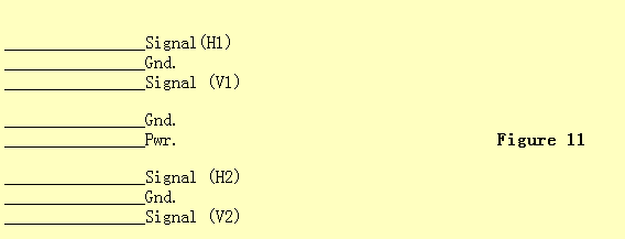
One of the many advantages of this layer stackup is the tightly coupled power-ground plane pair in the center. Typical layer spacing for this configuration might be 0.006"/0.006"/0.015"/0.006"/0.015"/0.006"/0.006." This configuration satisfies objectives 1 and 2, 3, and 5, but not 4. This is an excellent performing configuration with good signal intergity and is often preferred over the stack-up of Figure 10 because of the tightly coupled power/ground planes.
There is very little EMC advantage to use a board with more than eight layers. More that eight layers is usually used only when additional layers are required for signal trace routing. If six routing layers are needed, a ten-layer board should be used.