Industry Directory | Training Provider / Manufacturer's Representative / Equipment Dealer / Broker / Auctions / Consultant / Service Provider
Products, services, training & consulting for the assembly, rework & repair of electronic assemblies. BGA process experts. Manufacturers Rep, Distributor & Service Provider for Seamark/Zhuomao and Shuttle Star BGA Rework Stations.
Industry Directory | Manufacturer
PCB Global is a dedicated Prototype Quick Turn High Tech. PCB supplier - Quotes and orders can be processed 24/7/365 - free online quotation visit www.pcbglobal.com

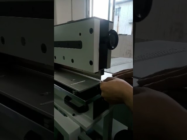
Structural precision Strict requirement pcb Depanel CWV-1M industrial made Specifications Strict requirement pcb depanelizer industrial made 1.PCB Protection 2.Calibration Blade Setting 3.All Speed Control By Human 4.More Accurating

1. Smooth cutting finish only by router cutting . 2. There is little distortion on PCB during cutting because using high-frequency spindle motor . It is 1 / 10 of pressing , 1 / 100 of breaking by hand . 3. One-touch program changeover . 4. Able to c
Electronics Forum | Fri Sep 01 05:29:01 EDT 2017 | mona0312
Hi, Recently, i found a company called "jlcpcb". It’s very cheap 10pcs boards. 1.2mm thick, 1-OZ copper, 6/6-mil outer (0.1525mm) just cost $2 Cheap price and lots of options regarding board thickness, colour, etc. None of my boards have ever had a
Electronics Forum | Mon Nov 07 16:34:55 EST 2005 | CW
If I am putting chip capacitors on a .063 FR4 board, what size package should we stay away from to avoid cracking? If I use 2 mil copper on the outside layers of a PCB, am I limited to what pitch of parts I can use? Specifically, will using 0603
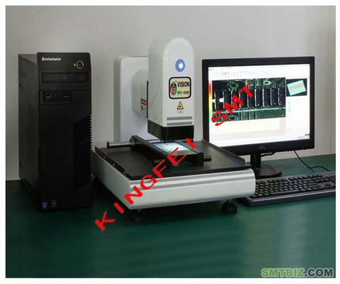
Used SMT Equipment | SPI / Solder Paste Inspection
Product Details of 3D SPI-6500 Thick Paste Measurement Instrument Product Functions 1, friendly programming interface 2, a variety of measurement methods 3, scan spacing adjustable 4, image 3D simulation function 5, independent 3D dynamic obser
Industry News | 2003-05-19 10:06:43.0
The PCB is available with a maximum panel size of 406-by-460mm and a minimum board thickness of 0.8mm.
Industry News | 2003-06-24 08:14:51.0
R/flex� 3850 laminate is produced in a range of copper and LCP thicknesses, just as the single-clad laminate, and is available in standard panel formats.

Parts & Supplies | Pick and Place/Feeders
N510017368AA BOLT Hexagon socket head cap screw M4X45-10.9 A2J (Trivalent) N510004786AA POST ETKRFT-25-250-1 N610018132AA COVER 0 MTNP000804AA JOINT KQ2W08-U01A N510020431AB CASE Mount Position Teach Jig Case N510018857AA BOLT Hexagon head bolt

Parts & Supplies | Circuit Board Assembly Products
1). FR-4 Material 2). 2 layer, 1.2mm thick 3). 5 oz copper weight. 4). LPI Green solder mask/White silk screen 5). Immersion gold over nickle
Technical Library | 2016-07-21 18:16:06.0
Achieving optimum high-frequency printed-circuit-board (PCB) performance is not simply a matter of specifying the best possible PCB material, but can be significantly impacted by PCB fabrication practices. In addition to appropriate circuit materials and circuit design configurations to meet target performance goals, a number of PCB material-related issues can affect final performance, including the use of soldermask, the PCB copper plating thickness, the conductor trapezoidal effect, and plating finish; understanding the effects of these material issues can help when fabricating high-frequency circuits for the best possible electrical performance.
Technical Library | 2019-07-17 17:56:34.0
The increased demand for electronic devices in recent years has led to an extensive research in the field to meet the requirements of the industry. Electrolytic copper has been an important technology in the fabrication of PCBs and semiconductors. Aqueous sulfuric acid baths are explored for filling or building up with copper structures like blind micro vias (BMV), trenches, through holes (TH), and pillar bumps. As circuit miniaturization continues, developing a process that simultaneously fills vias and plates TH with various sizes and aspect ratios, while minimizing the surface copper thickness is critical. Filling BMV and plating TH at the same time, presents great difficulties for the PCB manufactures. The conventional copper plating processes that provide good via fill and leveling of the deposit tend to worsen the throwing power (TP) of the electroplating bath. TP is defined as the ratio of the deposit copper thickness in the center of the through hole to its thickness at the surface. In this paper an optimization of recently developed innovative, one step acid copper plating technology for filling vias with a minimal surface thickness and plating through holes is presented.
Guillotine type V-cut PCB Cutting Machine Product Description 1. For internal strength generates during separation, Minimize it to value under 180uE ,to avoid solder crack or component damage 2. Able to separate edge of V-slot, minimum distance to
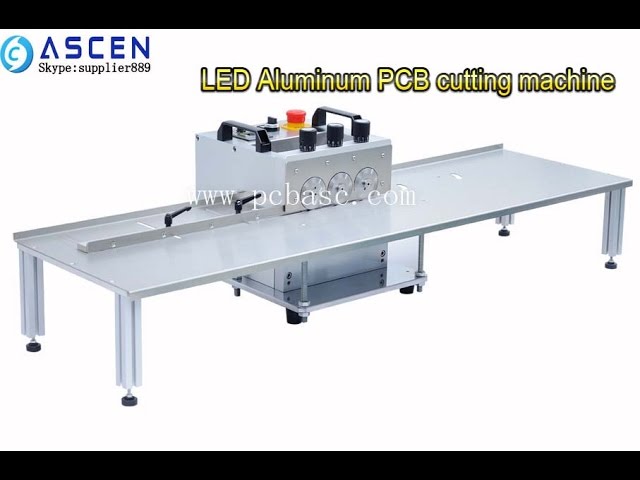
ASCEN specializing the PCB cutting machine, Please check: www.pcbasc.com www.aliexpress.com/store/1377040 led strip aluminum plate cutter free porn girl online v-cut pcb cutting doule layer pcb cutter depanelizing pcba plate machine aluminum pcb se
Training Courses | | | IPC-6012 Specialist (CIS)
The Certified IPC-6012 Specialist (CIS) training covers design, fabrication and inspection of rigid printed boards.
Training Courses | | | PCB Design Courses
The PCB design courses teach students the process, techniques and tools needed to design layout of printed circuit boards.
Events Calendar | Wed Apr 20 00:00:00 EDT 2022 - Wed Apr 20 00:00:00 EDT 2022 | ,
Virtual Course: Selection Criteria of Surface Finish for Next Generation PCB Technologies
Events Calendar | Mon Apr 23 00:00:00 EDT 2018 - Thu Apr 26 00:00:00 EDT 2018 | Shanghai, China
SMTA China East Conference 2018
Career Center | Shen Zhen, China | Management,Sales/Marketing
Working in GLORYPCB for 10 years.knowing electronic supply chain very well. especially for PCB PCBA assembly and other Electronic Manufacturing Service.Glorypcb is a professional electronic manufacturer located in Shenzhen with three facilities.offe
Career Center | Erode, Tamilnadu India | Engineering
Professional Summary 3+ years of experience in the PCB CAM engineering Exposure to FRONTLINE GENESIS 2000 Having exposure in UCAM Exposure to Create, Array & Panelize it for manufacturability Experienced in Creating impedance cou
Imagineering, Inc. | https://www.pcbnet.com/capabilities/fabrication/tolerances/
. A premium is charged for trace width/spacing less than .005″. For 0.5 oz. finished copper weight: the minimum trace width/space is 0.003″ For 1 oz
ASCEN Technology | https://www.ascen.ltd/Products/custom_automatic_machine/pcb_cutting_mach/387.html
length is 0 to 500mm and 0 to 360mm (blade length can be customized)blade height slight adjustment in 0 to 2mm, platform height adjustable in 0 to 50mm,to fit PCB of different thickness ,and solve the problem of different V-slot depth 3. Manually
Products, services, training & consulting for the assembly, rework & repair of electronic assemblies. BGA process experts. Manufacturers Rep, Distributor & Service Provider for Seamark/Zhuomao and Shuttle Star BGA Rework Stations.
Training Provider / Manufacturer's Representative / Equipment Dealer / Broker / Auctions / Consultant / Service Provider
1750 Mitchell Ave.
Oroville, CA USA
Phone: (888) 406-2830