Industry Directory | Manufacturer
Synova is an experienced manufacturer of innovative laser cutting systems for an extraordinary range of micro-machining and dicing applications.
Industry Directory | Other / Consultant / Service Provider / Manufacturer
We develop produce and supply innovative cost effective thermal control units to major Semiconductor Devices Manufacturers to test IC devices -LOW & HIGH Power devices for temp range -65°C to +200°C.

If you have boards requiring high tolerance mechanical dimension or odd shapes that traditional depaneling methods cannot handle. BEST Inc. provides laser depaneling services for printed circuit board manufacturers as well as EMS and OEMs. BEST’s nu

PCB depaneling (singulation) laser machines and systems have been gaining popularity over recent years. Mechanical depanaling/singulation is done with routing, die cutting, and dicing saw methods. However, as the boards get smaller, thinner, flexible
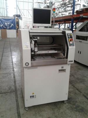
Used SMT Equipment | Depanelizers / Routers
Key Features Solution for stress free depanelization Fixture-based highly efficient dust vacuum system Clean and precise depanelization for densely populated PCBs Advanced image-processing software offers point-and-click operation fo
Industry News | 2011-12-14 15:35:33.0
Manufacturing processes, handling and printed circuit assembly (PCA) test can put a lot of mechanical stresses on packages, causing failures. As grid array packages get larger, identifying how to set safe levels for these steps becomes more difficult. A new quantitative test methodology within IPC/JEDEC-9707, Spherical Bend Test Method for Characterization of Board Level Interconnects, lets users determine how much strain packages can take before reliability degradation.
Industry News | 2018-08-29 19:35:22.0
IPC — Association Connecting Electronics Industries® invites engineers, researchers, academics, technical experts and industry leaders to submit abstracts for IPC High Reliability Forum to be held May 14–16, 2019 in Hanover (Baltimore), Md.
Technical Library | 2016-10-06 15:13:02.0
One of the methods gaining in popularity for singulating rigid/flex, rigid and flex circuit boards post assembly is through the use of laser routing. This method has the advantage of speed, positional accuracy, no tooling wear and lastly no induced mechanical stresses on components during the singulating process.
Technical Library | 2021-09-02 08:17:07.0
We are a professional manufacturer of PCB depaneling machines, which is workable for all boards, including flex and regid boards, v-scored boards and routed boards. Laser pcb depaneling is non-contact way without mechanical stress,this solution is good for modern precision PCB depaneling. It has below advantages: 1. No dust The production environment of the circuit board industry is carried out in the dust-free workshop. The traditional pcb depaneling equipment, such as blade moving type machine, will inevitably produce residues and micro powder, which will pollute the 10000 and 1000 class dust-free workshops and affect the conductivity of products. The UV laser PCB cutting machine is a vaporization processing process, which will not produce dust and is conducive to the conductivity of the product. 2. High cutting precision The processing gap of high-precision traditional processing equipment can not reach the gap width of less than 100 microns, which will cause certain damage to the lines on the edge or PCBA circuit board containing components. The focus spot of the laser cutting machine is small, and the ultraviolet cold processing mode has little thermal impact on the edge of the circuit board. The cutting position accuracy is less than 50 microns, and the cutting size accuracy is less than 30 microns, which will not affect the edge of the circuit board, and the precision is high. 3. No stress Traditional processing methods generally have V-grooves, which will cause certain damage to the board in the manufacturing process. The UV laser PCB cutting machine can directly cut the bare board without making V-grooves. In addition, the traditional processing methods directly use tools to act on the circuit board, especially the stamping method has a great impact on the circuit board, which is easy to cause board deformation. The laser cutting machine is a non-contact processing mode, which acts on the surface of the material through the high-energy beam, which will not cause the influence of stress and the deformation and damage of the circuit board. 4. For special-shaped cutting, it is easy to automate The UV laser PCB cutting machine can cut for any shape without replacing any props and fixtures, and without steel mesh. The same equipment can meet special-shaped and straight-line cutting, which is easy to realize assembly line automatic production and high flexibility. It is easy to improve production efficiency and save production process and production cycle. In particular, it can quickly and efficiently meet the needs of rapid proofing, directly import the drawing, and then locate the cutting. 5. High compatibility The UV laser PCB cutting machine can process the materials around the circuit board, such as PCB, FPC, covering film, pet, reinforcing board, IC, ultra-thin metal cutting, etc. it has strong practicability, is compatible with the processing of a variety of materials, is easy to operate, can be imported into the drawing, does not need to adjust any mechanical parts, and is easy to operate and maintain. 6. Good cutting edge effect The cutting edge is smooth and neat without burr. It can be processed and formed directly according to the size of the drawing, which is conducive to improving the yield of the product. It can be directly installed into the subsequent process without further processing. For more details about UV laser depaneling, please feel free to contact us. www.pcbdepanelingrouter.com

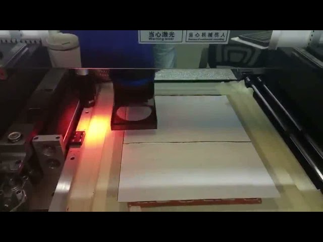
15W UV Laser Economic PCB Laser Depaneling System PCB Laser Depaneling System Specification: Laser solid-state UV laser Laser Wavelength 355nm Laser Source UV 15W@30KHz Positioning Precision ±2μm
Training Courses | | | PCB Rework and Hand Soldering Courses
The PCB rework and hand soldering courses courses cover techniques of rework and repair of PCBs, BGAs and other electronics assemblies, and teach fundamentals of soldering of electronics assemblies.
Career Center | San Jose, California USA | Engineering
Associate Mechanical Engineer The main role of the Associate Mechanical Engineer will be to design, develop, and build apparatuses and fixtures, which purpose will be to test and control our clients' manufacturing output. Each of these apparatuses a
Career Center | Houston, Texas USA | Engineering
Our South Houston client is looking to hire a Senior Mechanical Engineer on a direct hire basis. Job Summary: Perform the complete mechanical design required for both proprietary and non-proprietary projects. Assist with technical mechanical suppo
Career Center | , Abu Dhabi | Engineering,Management,Production,Sales/Marketing
• Strong technical leadership and decision-making skills; strong verbal and written communication skills to provide clear, crisp direction for key issue resolution; and good team skills to facilitate cross-functional cross -site team effectiveness.
Career Center | Rochester, New York USA | Engineering,Production,Sales/Marketing,Technical Support
Working Experience: Fairchild Semiconductor, South Portland, ME Package Simulation Co-op: Technology CAD Group (Mar.2002-Present) Thermal simulation for 40 lead fine pitch QSOP & 48 lead one die fine pitch QSOP: Created a 3D model
SMTnet Express, March 7, 2019, Subscribers: 31,716, Companies: 10,725, Users: 25,814 Effect of Encapsulation Materials on Tensile Stress during Thermo-Mechanical Cycling of Pb-Free Solder Joints Credits: DfR Solutions Electronic assemblies use a
PCB Libraries, Inc. | https://www.pcblibraries.com/forum/footprints-for-high-vibration-and-shock_topic2568_post10485.html
withstanding mechanical stress during operation. Ideally I'm looking for a standard or study relating component size and copper pad area to vibration/shock withstand