Industry Directory | Consultant / Service Provider / Manufacturer
Eureka Dry Tech's IPC/JEDEC J-Std-033c Ultra Low Humidity Dry Cabinets provides moisture/humidity controlled storage of MSD,PCB, IC packages. Drying technology trusted by millions in replacing baking, nitrogen & desiccant packs.
Industry Directory | Other / Consultant / Service Provider / Manufacturer
Taiwan Dry Tech Corp. manufacturer of Eureka Dry Tech Fast Super Dryers for moisture/humidity proof protective storage of PCB, MSD, IC packages, meets IPC/JEDEC J-STD-033 & IPC-1601.
New Equipment | Education/Training
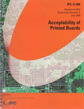
IPC A-600H Acceptability of Electronic Assemblies. The IPC-A-600, "Acceptability of Printed Boards " is the most widely used published specification on printed wiring boards. This specification has set the standard for rigid printed boards in terms o

New Equipment | Cleaning Equipment
WHAT IS THE PRECISION MATERIAL REMOVAL SYSTEM™ (PMRS)? The Precision Material Removal System (PMRS) is a multi-faceted system designed to be effectively used in three different applications: 1/ Conformal coating removal 2/ PCB Delamination
Electronics Forum | Thu Feb 12 20:42:10 UTC 2026 | SMTA-64387381
Is there any good reason not to print solder paste on DNPs on ENIG plated PCBs? Want to use a single stencil for building several BOM configurations on a common PCB. The in house design team is saying they do not allow printing on the DNP pads.
Industry News | 2011-01-12 17:48:44.0
GPD Global will highlight its Positive Cavity Displacement (PCD) Dispensing in Booth #6111 at the upcoming Automation and Technology West Expo (ATX), scheduled to take place February 8-10, 2011 at the Anaheim Convention Center in Anaheim, CA.
Industry News | 2012-03-05 14:26:45.0
GPD Global has been awarded a 2012 NPI Award in the category of Dispensing Equipment for its PCD Dispensing on the MAX Series Platform.


Technical Library | 2024-09-02 17:01:54.0
A printed circuit board (PCB) is an integral component of any electronic product and is among the most challenging components to recycle. While PCB manufacturing processes undergo generations of innovation and advancement with 21st century technologies, the recycling of PCBs primarily employs 1920's shredding and separation technologies. There is a critical need for alternative PCB recycling routes to satisfy the increasing environmental demands. Previous work has developed an environmentally benign supercritical fluid process that successfully delaminated the PCB substrates and separated the PCB layers. While this work was successful in delamination of the PCB substrates, further understanding is needed to maximize the interactions between the supercritical fluid and PCB for an optimal processing scenario. As such, this research presents an exploratory study to further investigate the supercritical fluid PCB recycling process by using supercritical carbon dioxide and an additional amount of water to delaminate PCB substrates. The focus of this study is to test delamination success at low temperature and pressure supercritical conditions in comparison to the previous studies. Furthermore, material characterization methods, such as differential scanning calorimetry, dynamic mechanical analysis, and Fourier transform infrared spectroscopy, are included to study the delaminating mechanisms. Results from the recycling process testing showed that the PCB substrates delaminated easily and could be further separated into copper foils, glass fibers and polymers. Surprisingly, the material characterization suggested that there were no significant changes in glass transition temperature, crosslink density, and FTIR spectra of the PCBs before and after the supercritical fluid process.
Technical Library | 2024-09-02 17:31:09.0
The cracking and delamination of printed circuit boards (PCB) during exposure to elevated thermal exposure, such as reflow and rework, have always been a concern for the electronics industry. However, with the increasing spread of Pb-free assembly into industries with lower volume and higher complexity, the occurrence of these events is increasing in frequency. Several telecom and enterprise original equipment manufacturers (OEMs) have reported that the robustness of their PCBs is their number one concern during the transition from SnPb to Pb-free product. Cracking and delamination within PCBs can be cohesive or adhesive in nature and can occur within the weave, along the weave, or at the copper/epoxy interface (see Figure 1). The particular role of moisture absorption and other PCB material properties, such as out of plane expansion on this phenomenon is still being debated.
This video describes the IPC A-600 training and certification program. The IPC A-600 specification is a set of acceptability specifications for printed circuit boards. These standards determine the acceptance and reject criteria for printed wiring bo
This video describes the IPC A-600 training and certification program. The IPC A-600 specification is a set of acceptability specifications for printed circuit boards. These standards determine the acceptance and reject criteria for printed wiring bo
Training Courses | | | IPC-600 Specialist (CIS)
The Certified IPC-600 Specialist (CIS) training targets quality assurance and acceptance of bare printed circuit boards.
Training Courses | | | IPC-600 Specialist (CIS)
The Certified IPC-600 Specialist (CIS) training targets quality assurance and acceptance of bare printed circuit boards.
Career Center | New Delhi, India | Engineering,Research and Development
I have 2 Years experience in SMT,THT and BGA components and 3+ years experience in total. Currently,working in a CMMi LEVEL 5 enviornment. I have been Working on various Panasonic series machines and fuji components. My work profile involves : 1. Si
Career Center | New Delhi, India | Engineering,Research and Development,Technical Support
I have 2 Years experience in SMT,THT and BGA components and 3+ years experience in total. Currently,working in a CMMi LEVEL 5 enviornment. I have been Working on various Panasonic series machines and fuji components. My work profile involves : 1. Si
Effects of an Appropriate PCB Layout and Soldering Nozzle Design on Quality and Cost Structure in Selective Soldering Processes If you don't see images, please visit online version at: http://www.smtnet.com/express/ Effects
| https://www.eptac.com/wp-content/uploads/2021/11/webinar_eptac_09_16_09.pdf
. The webinar will begin shortly. You will see the presentation slides on your computer monitor. To hear the audio, you must use a telephone. For Audio
| pcb-services-inc.com&gigaurl=https://precision-pcb-services-inc.com/blogs/news/ctdi-purchases-a-shuttle-star-sv550" target="_blank">https://precision-pcb-services-inc.com/blogs/news/ctdi-purchases-a-shuttle-star-sv550
CTDI purchases a Shuttle Star SV550! – Precision PCB Services, Inc. Search Log in or Create account Cart : 0 Menu Cart 0 Home Catalog Blog About us Log in Create account Search Precision PCB Services, Inc