If you have boards requiring high tolerance mechanical dimension or odd shapes that traditional depaneling methods cannot handle. BEST Inc. provides laser depaneling services for printed circuit board manufacturers as well as EMS and OEMs. BEST’s nu

PCB Laser Cutting Machine for Printed Circuit Boards,PCB Depaneling Parameter Technical parameters Main body of laser 1000mm*940mm *1520 mm
Industry News | 2015-10-21 17:02:27.0
Product lead time reductions and increased capabilities for EMS providers and board shops
Industry News | 2003-06-24 08:14:51.0
R/flex� 3850 laminate is produced in a range of copper and LCP thicknesses, just as the single-clad laminate, and is available in standard panel formats.
Technical Library | 2019-09-11 23:33:04.0
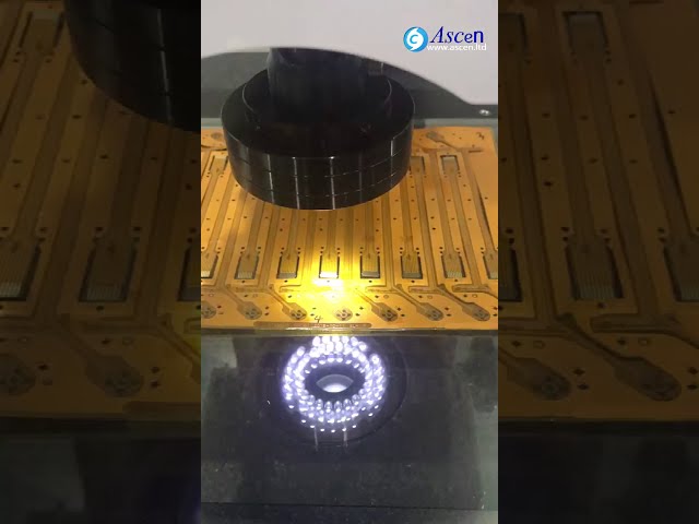
There are numerous techniques to singulate printed circuit boards after assembly including break-out, routing, wheel cutting and now laser cutting. Lasers have several desirable advantages such as very narrow kerf widths as well as virtually no dust, no mechanical stress, visual pattern recognition and fast set-up changes. The very narrow kerf width resulting from laser ablation and the very tight tolerance of the cutting path placement allows for more usable space on the panel. However, the energy used in the laser cutting process can also create unwanted products on the cut walls as a result of the direct laser ablation. The question raised often is: What are these products, and how far can the creation of such products be mitigated through variation of the laser cutting process, laser parameters and material handling? This paper discusses the type and quantity of the products found on sidewalls of laser depaneled circuit boards and it quantifies the results through measurements of breakdown voltage, as well as electrical impedance. Further this paper discusses mitigation strategies to prevent or limit the amount of change in surface quality as a result of the laser cutting process. Depending on the final application of the circuit board it may prompt a need for proper specification of the expected results in terms of cut surface quality. This in turn will impact the placement of runs and components during layout. It will assist designers and engineers in defining these parameters sufficiently in order to have a predictable quality of the circuit boards after depaneling.
Technical Library | 2018-03-28 14:54:36.0
Six decades of legacy experience makes the specification and production of screens and masks to produce repeatable precision results mostly an exercise in matching engineering needs with known ink and substrate performance to specify screen and stencil characteristics. New types of functional and electronic devices, flex circuits and medical sensors, industrial printing, ever finer circuit pitch, downstream additive manufacturing processes coupled with new substrates and inks that are not optimized for the rheological, mechanical and chemical characteristics for the screen printing process are becoming a customer driven norm. Many of these materials do not work within legacy screen making, curing or press set-up parameters. Many new materials and end uses require new screen specifications.This case study presents a DOE based method to pre-test new materials to categorize ink and substrate rheology, compatibility and printed feature requirement to allow more accurate screen recipes and on-press setting expectations before the project enters the production environment where time and materials are most costly and on-press adjustment methods may be constrained by locked, documented or regulatory processes, equipment limitations and employee experience.

https://www.ascen.ltd/Products/PCB_board_assembly_system/vision_measurin/507.html Vision Measuring Machine and image measuring instrument can be used for dimensional accuracy measurement of various molds, aircraft, automobile, mobile phone, computer,
Events Calendar | Wed Sep 16 18:30:00 UTC 2020 - Wed Sep 16 18:30:00 UTC 2020 | ,
DFM Panel Discussion for PCB Design, Fabrication, and Assembly
Career Center | Racine, Wisconsin USA | Engineering,Maintenance,Production,Technical Support
We are currently seeking a SMT Process Technician to join our already strong team in a state-of-the-art SMT/PTH facility, only 5 years old. This position will be responsible for all aspects of printed circuit board assembly, from programming of eq
Career Center | Racine, Wisconsin USA | Engineering
Cree currently has a job vacancy for an SMT Process Technician in our Lighting Manufacturing facility in Racine, Wisconsin. Summary: This person will be a primary contributor to the startup of a new SMT production line for LED PCB Assembly. This
Career Center | Cavite, Philippines | Maintenance,Production,Technical Support
January 15- 2013 to Prsent :Maintenace Technician National Agriculture Development Company Haradh Project 2557 Riyadh 11461, Saudi Arabia Responsibilities 1. Daily checking of Electrical Panels 2. Install Main power for
SMTnet Express, April 10, 2014, Subscribers: 22635, Members: Companies: 13857, Users: 36009 Solar Panel Design Decision and General Information Sheet Alexander L Carrere; iSAT Group This paper is meant to be a guide and a reference to new and old
SMTnet Express, September 14, 2017, Subscribers: 30,799, Companies: 10,725, Users: 23,800 The Relationship Between Energy-Resource Depletion, Climate Change, Health Resources and the Environmental Kuznets Curve: Evidence From the Panel of Selected
ASYMTEK Products | Nordson Electronics Solutions | https://www.nordson.com/en/divisions/select/soldering-processes/process-troubleshooting-guide
of solder joint formation. Critical factors directly affecting solder joint quality include process parameters, printed circuit board assembly, board fabrication techniques, and board design
| https://www.smtfactory.com/SMT-Solution-for-Solar-Panel-Manufacturing-id41032627.html
. For the Solar Panel Manufacturing, We can provide full SMT Line Solution and DIP Line Solution. Following are the base SMT Solution for your reference. SMT Process