Industry Directory | Manufacturer
R&D, production and sales of chemicals, equipment and related materials used in the production of PCB
Industry Directory | Manufacturer
Founded in 1985, Amitron Corporation has grown into one of the largest and most experienced printed circuit board manufacturers in North America. We are world leaders in thermal management technology development.

New Equipment | Fabrication Services
Hitechpcb is a professional manufacturer of copper based printed circuit board (PCB). We produce metal-based MCPCB, aluminum substrate and copper substrate PCBs. with short delivery time, strict quality and excellent service. What is Copper Based PCB

New Equipment | Fabrication Services
Hitech is a professional heavy copper pcb, thick copper pcb board manufacturer, PCB power supplier from China, we have been associated with heavy copper pcb plating since 2000 and we have won good reputation in this industry. If you have customized
Industry News | 2019-01-30 08:13:02.0
The SMTA is pleased to announce the Best Papers from SMTA International 2018. As speakers at SMTA International, individuals make contributions to the industry by sharing their research and findings. For these exceptional achievements, a cash award and plaque are given to all winners.
Industry News | 2017-11-13 13:38:37.0
IPC's Validation Services Program has awarded an IPC-4101 Qualified Products Listing (QPL) to Ventec International Group, a global electronics material manufacturing company headquartered in Suzhou, China.
Technical Library | 2019-06-20 00:09:49.0
It is well known that during service the layer of Cu6Sn5 intermetallic at the interface between the solder and a Cu substrate grows but the usual concern has been that if this layer gets too thick it will be the brittleness of this intermetallic that will compromise the reliability of the joint, particularly in impact loading. There is another level of concern when the Cu-rich Cu3Sn phase starts to develop at the Cu6Sn5/Cu interface and an imbalance in the diffusion of atomic species, Sn and Cu, across that interface results in the formation at the Cu3Sn/Cu interface of Kirkendall voids, which can also compromise reliability in impact loading. However, when, as is the case in some microelectronics, the copper substrate is thin in relation to the volume of solder in the joint an overriding concern is that all of the Cu will be consumed by reaction with Sn to form these intermetallics.This paper reports an investigation into the kinetics of the growth of the interfacial intermetallic, and the consequent reduction in the thickness of the Cu substrate in solder joints made with three alloys, Sn-3.0Ag-0.5Cu, Sn-0.7Cu-0.05Ni and Sn-1.5Bi-0.7Cu-0.05Ni.
Technical Library | 2017-04-20 13:51:14.0
The one constant in electronics manufacturing is change. Moore's Law, which successfully predicted a rate of change at which transistor counts doubled on Integrated Circuits (ICs) at lower cost for decades, is ceding to be an appropriate prediction tool. Increasing technical and economic requirements, deriving from the semiconductor environment, are cascaded down to the printed circuit and in particular to the IC substrate manufacturers. This is both a challenge and an opportunity for IC Substrate manufacturers, when dealing with the demands of the packaging market. (...)This paper introduces two new electroless copper baths developed for IC substrates manufacturing based on Semi Additive Process (SAP) technology (hereafter referred to as E'less Copper IC) and HDI production (hereafter referred to as E'less Copper HDI) and optimized for high throw into BMVs. An introduction to reliable throwing power measurement methods based on scanning electron microscope (SEM) is given, followed by a compilation and discussion of key performance criteria for each application, namely throwing power, copper adhesion on the substrate, dry film adhesion and reliability.

Hitechpcb is a professional manufacturer of copper based printed circuit board (PCB). We produce metal-based MCPCB, aluminum substrate and copper substrate PCBs. with short delivery time, strict quality and excellent service. What is Copper Based PCB
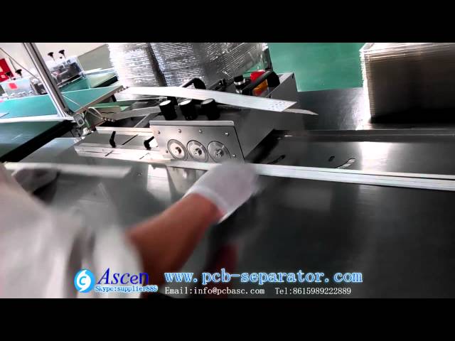
http://www.pcb-separator.com ??????????? ???????? ????/?????/V??????????????/LED depaneling equipment/separator/LED separator manufacturer/supplier/
Events Calendar | Tue Jul 02 18:30:00 UTC 2024 - Tue Jul 02 18:30:00 UTC 2024 | ,
Europe Chapter Webinar: "Back-to-Basics" SMT Assembly
Events Calendar | Thu Apr 15 18:30:00 UTC 2021 - Thu Apr 15 18:30:00 UTC 2021 | ,
Auburn University Student Chapter Event: Get Hired in Electronics Industry
Career Center | Rochester, New York USA | Engineering,Production,Quality Control,Technical Support
Having gained strong knowledge of populating printed circuit boards through 7 years experience, including experience with copper plated ceramic substrate fabrication. Additionally, I�ve addressed numerous technical issues of manufacturing circuit boa
Career Center | Toronto,, Ontario Canada | Engineering,Research and Development
DEBTANU BASU 40 Fountain Head Road Toronto, ON M3J2V1 (416) 514 0619 Cell: 416 258 7488 E-mail: debtanubasu@aol.com With more than six years of experience in the field of flip chip technologies seeking a challenging technical position in the field
SMTnet Express, April 20, 2017, Subscribers: 30,402, Companies: 10,575, Users: 23,153 High Throw Electroless Copper - Enabling new Opportunities for IC Substrates and HDI Manufacturing Tobias Sponholz, Lars-Eric Pribyl, Frank Brüning, Robin Taylor
SMTnet Express, November 22, 2017, Subscribers: 31,034, Companies: 10,792, Users: 24,082 Factors Affecting the Adhesion of Thin Film Copper on Polyimide David Ciufo, Hsin-Yi Tsai and Michael J. Carmody; Intrinsiq Materials Inc. The use of copper
| http://etasmt.com/cc?ID=te_news_industry,26961&url=_print
. And our epoxy resin and BT are all organic materials. 2. Inorganic materials: ① Aluminum substrate: The aluminum substrate is a metal-based copper clad laminate with good heat dissipation function
ASYMTEK Products | Nordson Electronics Solutions | https://www.nordson.com/en/divisions/sonoscan/support/application-notes/1066-voids-in-solder
. The image was generated at 50 MHz by focusing through the copper base to the copper base/ceramic substrate interface. Result The black areas observed in the substrate regions (multi-colored areas