New Equipment | Soldering - Other
ASCEN solder dross separator used in the PCB electronic industry,it is designed to recover pure tin and solder dross from working impurities oxides generated from the wave soldering with lead or lead free process.This tin slag recycling machine not o

JUKI JM-20 Hybrid Placement Machine Max PCB:410×560mmComponent Size:0603~50mmPlace Speed:15,500 CPHProduct description: JUKI JM-20 Multi Task Platform Hybrid Placement Machine, Max PCB:410×560mm, Component Size:0603~50mm, Place Speed:15,500 CPH

Used SMT Equipment | AOI / Automated Optical Inspection
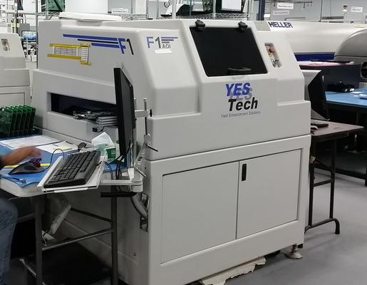
YesTech YTV-F1 Automated PCB Inspection System >Multi-function all purpose In-Line system • (2) Top-down Cameras; Incl. (1) High Magnification • (4) side viewing cameras • LED top light, bi-color multiangle LED lighting •
Used SMT Equipment | AOI / Automated Optical Inspection
YesTech YTV-F1 Automated PCB Inspection System >Multi-function all purpose In-Line system • (2) Top-down Cameras; Incl. (1) High Magnification • (4) side viewing cameras • LED top light, bi-color multiangle LED lighting •
Industry News | 2018-10-18 08:53:06.0
Mixed process of SMT reflow oven
Industry News | 2012-11-02 09:04:14.0
IPC and SMTA jointly announce the agenda for Session 5 of the High-Reliability Cleaning and Coating Conference, scheduled to take place November 13-15, 2012 at the Crowne Plaza Hotel – O’Hare in Chicago, IL.
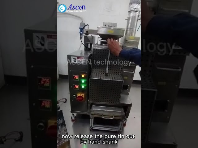
ASCEN solder dross separator used in the PCB electronic industry,it is designed to recover pure tin and solder dross from working impurities oxides generated from the wave soldering with lead or lead free process.This tin slag recycling machine not o
500,000 components per hour Maximum Board Size: 18” x 20” (457mm x 508mm) Clearance: 2” (50mm) top and bottom Minimum Component Size: 0201; 01005 with high magnification option
Events Calendar | Wed May 12 18:30:00 UTC 2021 - Wed May 12 18:30:00 UTC 2021 | ,
Joint Chapter Meeting: Photonic Soldering
for missing balls (BGA's - figure 23), or bent or missing l
| https://www.eptac.com/ask/gullwing-lead-deformation/
% of the diameter, width, or thickness of the lead.” So if the leads are damaged or bent more than 10% of the diameter, width, or thickness of the lead, they cannot be used
1st Place Machinery Inc. | http://www.firstplacemachinery.com/first_place_smt_pcb_aoi_mvp.html
. System can inspect SMT components pre-or post solder for presence / absence and placement verification (x,y,and theta ) polarity, solder fillet, bridging, solder opens, insufficient fillets, excess solder, and lifted leads