Industry Directory | Other / Manufacturer
ISO certified global manufacturer and supplier of light-curable adhesives, coatings, oligomers, dispense systems, light-curing equipment, and technical consulting for the industrial, medical, and electronics industries.
Industry Directory | Manufacturer
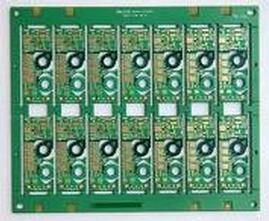
a pcb manufacturer in China specializing in multi-layer pcbs that meet RoHs, UL, IPC standards.
New Equipment | Rework & Repair Services
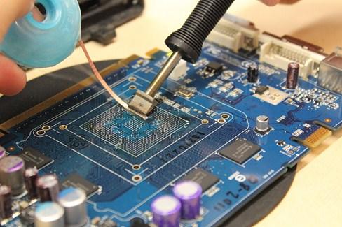
Your BEST Source For High Quality Industry-Leading BGA Repair Service BEST provides industry-leading solutions for Ball Grid Array BGA Repair Services and other grid array device reworks. Our engineers have developed better processes to make our BGA

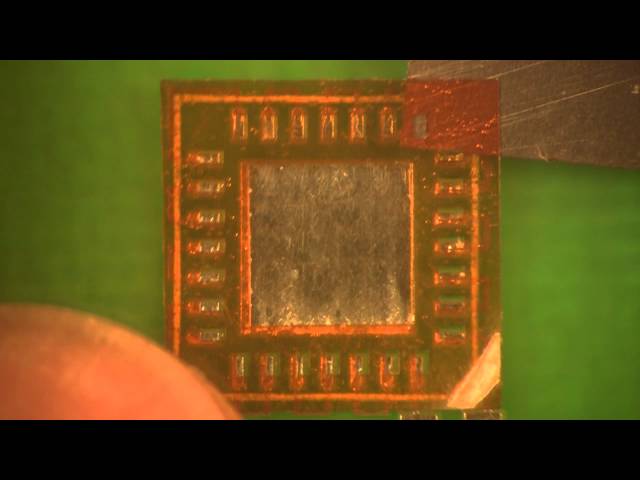
New Equipment | Rework & Repair Services
Reliable LGA Rework Services to Rescue Your Project BEST is your source for LGA rework services. We can optimize our processes to make sure voiding is minimized and the interconnection to all of the IO meets the IPC classification for the assembly.

Used SMT Equipment | Soldering - Wave
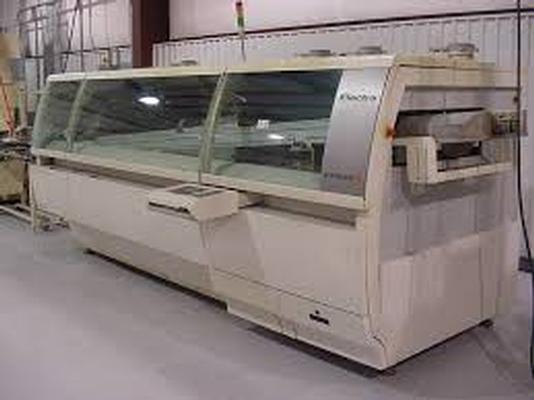
Options: (1) IR-preheating, bottom side segmented pin/chain and roller conveyor for versaflow with double soldering module programmable conveyor width adjust (4) convection preheating top side automatic solder wire feeder, solder
Used SMT Equipment | Soldering - Wave
BASE-EC Electra Base Machine 1 CE-WS CE Compliance 1 RGDI-EC Rigid Intermix Fingers 1 FMSK-EC Finger Mask 2 FANS-WS Cooling Fans Option 1 VEC-EC Vecta Heater 2 IR-EC Infrared Heater 1 TOPIR-EC Top Infrared Heater 1 O2-WS OptiFlux II 1 O2SLCT
Industry News | 2015-10-21 17:02:27.0
Product lead time reductions and increased capabilities for EMS providers and board shops
Industry News | 2017-03-31 12:29:11.0
BEST installs and brings Up mass rework machine capability to reduce costs and increase the turnover of boards requiring lots of parts change outs.
Technical Library | 1999-05-06 13:38:45.0
This paper traces the key steps that led to the invention of the integrated circuit (IC). The first part of this paper reviews the steady improvements in the performance and fabrication of single transistors in the decade after the Bell Labs breakthrough work in 1947. It sketches the various developments needed to produce a practical IC. In addition, the more advanced processes such as diffusion, oxide masking, photolithography, and epitaxy, which culminated in the planar process, are summarized.
Technical Library | 2021-11-03 17:05:39.0
Additively printed circuits provide advantages in reduced waste, rapid prototyping, and versatile flexible substrate choices relative to conventional circuit printing. Copper (Cu) based inks along with intense pulsed light (IPL) sintering can be used in additive circuit printing. However, IPL sintered Cu typically suffer from poor solderability due to high roughness and porosity. To address this, hybrid Cu ink which consists of Cu precursor/nanoparticle was formulated to seed Cu species and fill voids in the sintered structure. Nickel (Ni) electroplating was utilized to further improve surface solderability. Simulations were performed at various electroplating conditions and Cu cathode surface roughness using the multi-physics finite element method. By utilizing a mask during IPL sintering, conductivity was induced in exposed regions; this was utilized to achieve selective Ni-electroplating. Surface morphology and cross section analysis of the electrodes were observed through scanning electron microscopy and a 3D optical profilometer. Energy dispersive X-ray spectroscopy analysis was conducted to investigate changes in surface compositions. ASTM D3359 adhesion testing was performed to examine the adhesion between the electrode and substrate. Solder-electrode shear tests were investigated with a tensile tester to observe the shear strength between solder and electrodes. By utilizing Cu precursors and novel multifaceted approach of IPL sintering, a robust and solderable Ni electroplated conductive Cu printed electrode was achieved.
This video describes the BEST BGA rework and BGA rework services capabilities. What is described in this movie are the people, processes and tools unique to BEST and how that impacts its customers. The advanced equipment set including multiple refl
Career Center | Space Coast, Florida USA | Engineering,Research and Development
Board Level Assembly BGA Expert! We are in need of an Electronic Packaging or Advanced Manufacturing Engineer to work with the Advanced Manufacturing Technology Group of a major Florida based Communications company. Support IR&D and Program activit
Career Center | Melbourne, Florida USA | Engineering
Advanced Manufacturing Technology Position Description Job Description: AMT Engineer � Level 4 Support IR&D and Program activities Division wide working on the development, qualification, and implementation of electronic packaging technologies, wi
Career Center | San Jose, California USA | Accounting/Finance,Engineering,Human Resources,Production,Technical Support
Contract Recruiter Services � Technical Sourcing, Accurate Job Req Development, On-Boarding Process, Happy Hiring Managers/New Employees Roger Sill - Recruiting Biography Phone 408.926.6212 Position: Senior Recruiter (Contract); or Lead Recruit
PCB Libraries, Inc. | https://www.pcblibraries.com/forum/advice-for-solder-mask-paste-mask-layers_topic484_page1.html
Advice For Solder Mask & Paste Mask Layers - PCB Libraries Forum Forum Home > PCB Footprint Expert > Questions & Answers New Posts FAQ Search Events Register Login Advice For Solder Mask
Imagineering, Inc. | https://www.pcbnet.com/blog/what-is-solder-mask-color-selecting-the-right-option-for-your-product/
. This creates the characteristic patterns commonly seen on a printed circuit board. For the purposes of electronic design automation, the solder mask is treated as an additional layer of the circuit board and is described as a Gerber file similar to that of copper and silkscreen layers