
Industry Directory | Consultant / Service Provider / Media / Publisher / Online Resource / Other
PCB Libraries' "Footprint Expert" suite uses CAD LEAP(tm) Technology to greatly simplify footprint and 3D STEP model creation; it is used by tens of thousands of PCB designers and engineers all over the world.
Contract electronics design and manufacturing service provider. ISO-9002 certified and IPC Class II and III capable. Advanced SMT packages including uBGA and 0201 components. Full testing, X-ray inspection, and automated conformal coating.
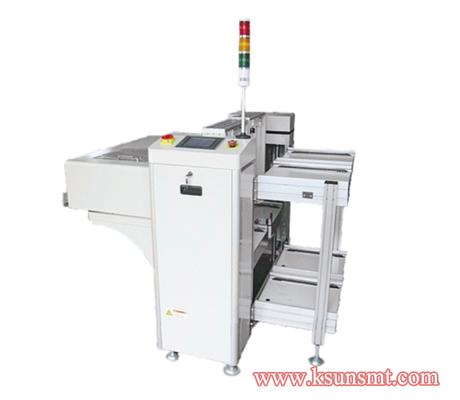
New Equipment | Board Handling - Conveyors
product instruction ※PLC control system, Working is stably and reliably ※Easy to operate touch screen control interface ※the pneumatic clamps of top and bottom three point provided for the magazine alignment ※Electric pushing board design ca

New Equipment | Board Handling - Conveyors
product instruction ※PLC control system, Working is stably and reliably ※Easy to operate touch screen control interface ※the pneumatic clamps of top and bottom three point provided for the magazine alignment ※Electric pushing board design ca
Electronics Forum | Thu Oct 03 18:45:56 EDT 2002 | davef
Get started with an "On-Board Forum" [blue bar an inch down from the top of the page] moderated by Jeff Schake at DEK that was a discussion focused on stencil printing issues with 0201 technology. Chris: Are you putting 0201 on flex? If so, sounds
Electronics Forum | Fri Oct 04 11:25:49 EDT 2002 | Bob Willis
If you want some additional material on 0201 design and assembly the SMART Group Committee produced one of its Charity Reports with all the money raised going to the Red Cross USA September 11th Appeal. You can get it from the SMTA Main office, it fe
Used SMT Equipment | Screen Printers
DEK Horizon 03i automatic stencil printer Specification : DEK Horizon 03i High Precision Automatic Solder Paste Printer designed for high precision steel mesh printing or stencil printing in SMT industry. Printing PCB size: 50x50mm to 508x510mm;

Used SMT Equipment | Chipshooters / Chip Mounters
Maximum speed up to 42,000CPH (Optimum) and 29,000CPH (IPC9850) With maximum speed up to 42,000CPH (Optimum) and 29,000CPH (IPC9850), the RS-1 is designed for maximum throughput. The RS-1 supports components from 0201 metric (008004") up to 74m
Industry News | 2016-06-22 15:33:28.0
Based on its recent analysis of the surface mount technology (SMT) reflow soldering equipment market, Frost & Sullivan recognizes Heller Industries, Inc. with the 2016 Global Frost & Sullivan Award for Growth Excellence Leadership. Heller Industries has made remarkable improvements to its product and technology portfolios over the last 10 years to emerge a top participant in the SMT reflow soldering equipment market.
Industry News | 2017-01-26 19:53:00.0
GPD Global will exhibit in Booth 2933 at the upcoming IPC APEX EXPO 2017 scheduled to take place February14-16, San Diego Convention Center. GPD Global will officially launch its new, fully automated dispense platform, Hyperion, and a new, low cost conformal coating system.
 – pn 51305433.jpg)
Parts & Supplies | Pick and Place/Feeders
0402 Ceramic Blade Nozzle (3030) – p/n 51305433 You might ask, “What’s the difference between this nozzle and the older conical 0402 ceramic nozzle?” Simply put, we think this latest design is a far superior option. Here&
 51305434_1.jpg)
Parts & Supplies | Pick and Place/Feeders
0603 Ceramic Blade Nozzle 3040 51305434 We were so impressed with the new long-life ceramic 0402 nozzle (#3030) we launched earlier in 2014 that we decided to follow it up with an 0603 version! Now customers can reap the benefits of our ESD-Safe ce
Technical Library | 2023-05-02 19:03:34.0
The demand for 0201 components in consumer products will increase sharply over the next few years due to the need for miniaturization. It is predicted that over 20 billion 0201 components will be used in more than one billion cell phones worldwide by the year 2003. Therefore, research and development on 0201 assembly is becoming a very hot topic. The first step to achieve a successful assembly process is to obtain a good PCB design for 0201 packages. This paper presents the data and criteria of PCB design for 0201 packages, including the pad design for 0201 components, and the minimum pad spacing or component clearance between 0201 components or between 0201 and other components. A systematic study on pad design and pad spacing was undertaken, using two test vehicles and three Design of Experiments (DOEs). In the first DOE, 2 out of 18 types of 0201 pad designs were selected based on process yield. The second DOE was focused on pad spacing, including 10mil, 8mil, 6mil and 4mil. The third experiment was final optimization, using two types of optimized pad designs with 10mil, 8mil and 6mil pad spacing. Through the above experiments, the design guideline for PCB layout for 0201 packages and the assembly process capability are identified.
Technical Library | 2023-05-02 19:06:43.0
As 0402 has become a common package for printed circuit board (PCB) assembly, research and development on mounting 0201 components is emerging as an important topic in the field of surface mount technology for PWB miniaturization. In this study, a test vehicle for 0201 packages was designed to investigate board design and assembly issues. Design of Experiment (DOE) was utilized, using the test vehicle, to explore the influence of key parameters in pad design, printing, pick-andplace, and reflow on the assembly process. These key parameters include printing parameters, mounting height or placement pressure, reflow ramping rate, soak time and peak temperature. The pad designs consist of rectangular pad shape, round pad shape and home-based pad shape. For each pad design, several different aperture openings on the stencil were included. The performance parameters from this experiment include solder paste height, solder paste volume and the number of post-reflow defects. By analyzing the DOE results, optimized pad designs and assembly process parameters were determined.

The PCB Footprint Expert is a powerful CAD library development tool powered by our own proprietary CAD LEAP Technology (Libraries Enhanced with Automated Preferences). It is packed with very powerful advanced library management features that cuts foo
Training Courses | | | PCB Design Courses
The PCB design courses teach students the process, techniques and tools needed to design layout of printed circuit boards.
Training Courses | | | PCB Assembly Courses
The PCB assembly courses provide knowledge of different processes and equipment used in TH and SMT assembly of printed circuit boards.
Events Calendar | Thu Mar 18 00:00:00 EDT 2021 - Thu Mar 18 00:00:00 EDT 2021 | ,
India Chapter Webinar: PCBA Process Qualifications
Events Calendar | Mon Jun 10 00:00:00 EDT 2024 - Mon Jun 10 00:00:00 EDT 2024 | Carlsbad, California USA
San Diego Chapter In-Person Event: IPC J-STD-001 Compliant Solder Pattern Calculations for DFA
Career Center | San Jose, CA, California USA | Engineering,Production,Research and Development
Senior PCB Designer: Want to be part of an exciting pre-IPO enterprise B2B company working on the cutting edge of internet-of-things, artificial intelligence & agents, blockchain, and manufacturing technology? This well-funded venture-backed co
Career Center | Clarksburg, Maryland USA | Engineering,Management,Research and Development,Technical Support
We are currently seeking a Senior Manufacturing Engineer for our Clarksburg, Maryland location. The candidate must be driven with a strong ability to multi-task under pressure. Responsibilities: The successful candidate will be responsible for:
Career Center | Newport Beach, California USA | Engineering,Management,Production
KEVIN RAGER P.O.BOX 7878, NEWPORT BEACH, 949 922 8997, KEVIN.RAGER@EDA-INC.US OBJECTIVE I am trying to find a consistent work flow that provides mentally challenging yet stimulating experiences in design and prototype development. EXPERIENCE 1997
| https://www.eptac.com/blog/3-common-pcb-design-mistakes
3 Common PCB Design Mistakes Looking for solder training standards, manuals, kits, and more? Visit soldertraining.com Training Training Materials Locations Resources Ask Helena
PCB Libraries, Inc. | https://www.pcblibraries.com/forum/topic43&OB=DESC.html
Mask opening for 0201 parts - PCB Libraries Forum Forum Home > Libraries > Footprints / Land Patterns > Expedition New Posts FAQ Search Events Register Login Mask opening for 0201 parts


winsouce.jpg)