Industry Directory | Manufacturer
professional manufacturer of pcb
Industry Directory | Consultant / Service Provider / Manufacturer
Specializing in electronic circuit board assembly services. Various capabilities include engineering, assembly, designing, prototyping,supply chain management, testing, documentation, rework, repair and soldering. On-time delivery
New Equipment | Rework & Repair Services
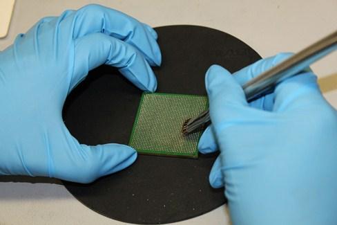
BGA Reballing Services BEST provides BGA reballing services for your plastic-, ceramic- and metalbodied components down to 0.3mm pitch. We have the ability to develop the BGA reballing process you want with a variety of deballing methods and machine

New Equipment | Rework & Repair Services
BGA Rework Service - Your BEST Source For High Quality BGA Rework Services BEST provides industry-leading solutions for BGA and other grid array device reworks. Our engineers have developed better processes to make BGA Rework Service more repeatable

Used SMT Equipment | Flexible Mounters
Product Name: Samsung CP45FV multi-function chip mounter Product number: CP45FV Detailed product introduction Samsung CP45FV multi function placement: Mounting head: 6 mounting head Servo system: servo motor drive X, Y shaft - Z axis shift drive
Used SMT Equipment | SMT Equipment
Product Name: Samsung CP45FV multi-function chip mounter Product number: CP45FV Detailed product introduction Samsung CP45FV multi function placement: Mounting head: 6 mounting head Servo system: servo motor drive X, Y shaft - Z axis shift drive
Industry News | 2013-09-03 11:52:21.0
BEST's EZReball(TM) reballing preforms now are available as standard in 3 business days. Expedited packs are in available in 24 hours to help you with your reballing projects
Technical Library | 2020-10-27 02:07:31.0
For companies that choose to take the Pb-free exemption under the European Union's RoHS Directive and continue to manufacture tin-lead (Sn-Pb) electronic products, there is a growing concern about the lack of Sn-Pb ball grid array (BGA) components. Many companies are compelled to use the Pb-free Sn-Ag-Cu (SAC) BGA components in a Sn-Pb process, for which the assembly process and solder joint reliability have not yet been fully characterized. A careful experimental investigation was undertaken to evaluate the reliability of solder joints of SAC BGA components formed using Sn-Pb solder paste. This evaluation specifically looked at the impact of package size, solder ball volume, printed circuit board (PCB) surface finish, time above liquidus and peak temperature on reliability. Four different BGA package sizes (ranging from 8 to 45 mm2) were selected with ball-to-ball pitch size ranging from 0.5mm to 1.27mm. Two different PCB finishes were used: electroless nickel immersion gold (ENIG) and organic solderability preservative (OSP) on copper. Four different profiles were developed with the maximum peak temperatures of 210oC and 215oC and time above liquidus ranging from 60 to 120 seconds using Sn-Pb paste. One profile was generated for a lead-free control. A total of 60 boards were assembled. Some of the boards were subjected to an as assembled analysis while others were subjected to an accelerated thermal cycling (ATC) test in the temperature range of -40oC to 125oC for a maximum of 3500 cycles in accordance with IPC 9701A standard. Weibull plots were created and failure analysis performed. Analysis of as-assembled solder joints revealed that for a time above liquidus of 120 seconds and below, the degree of mixing between the BGA SAC ball alloy and the Sn-Pb solder paste was less than 100 percent for packages with a ball pitch of 0.8mm or greater. Depending on package size, the peak reflow temperature was observed to have a significant impact on the solder joint microstructural homogeneity. The influence of reflow process parameters on solder joint reliability was clearly manifested in the Weibull plots. This paper provides a discussion of the impact of various profiles' characteristics on the extent of mixing between SAC and Sn-Pb solder alloys and the associated thermal cyclic fatigue performance.
Technical Library | 2023-07-25 16:50:02.0
Some of the new handheld communication devices offer real challenges to the paste printing process. Normally, there are very small devices like 01005 chip components as well as 0.3 mm pitch uBGA along with other devices that require higher deposits of solder paste. Surface mount connectors or RF shields with coplanarity issues fall into this category. Aperture sizes for the small devices require a stencil thickness in the 50 to 75 um (2-3 mils) range for effective paste transfer whereas the RF shield and SMT connector would like at least 150 um (6 mils) paste height. Spacing is too small to use normal step stencils. This paper will explore a different type of step stencil for this application; a "Two-Print Stencil Process" step stencil. Here is a brief description of a "Two-Print Stencil Process". A 50 to 75 um (2-3 mils) stencil is used to print solder paste for the 01005, 0.3 mm pitch uBGA and other fine pitch components. While this paste is still wet a second in-line stencil printer is used to print all other components using a second thicker stencil. This second stencil has relief pockets on the contact side of the stencil any paste was printed with the first stencil. Design guidelines for minimum keep-out distances between the relief step, the fine pitch apertures, and the RF Shields apertures as well relief pocket height clearance of the paste printed by the first print stencil will be provided.

Events Calendar | Wed Mar 17 18:30:00 UTC 2021 - Wed Mar 17 18:30:00 UTC 2021 | ,
India Chapter Webinar: PCBA Process Qualifications
Career Center | , Israel | Engineering,Maintenance,Technical Support
I was born on June , 1972 in Khmelnitsky city , Ukraine . I am male. From 1979 to 1987 I was studying at secondary school #7, having finished which I entered the Technical College of Khmelnitsky in specialty Machine Tools with Computer Numeric Contr
Heller Industries Inc. | https://hellerindustries.com/wp-content/uploads/2018/07/last-will-of-bga-void.pdf
sizes and pitches are listed in Table 2 together with the Practical Components part numbers. 166 Table 2. Components Characteristics Part Size Pitch Part Number BGA56 6x6 mm 0.5 mm A-CABGA56- .5mm-6mm-DC BGA256 17x17 mm 0.8 mm A-CABGA256- 1.0mm-17mm- DC


winsouce.jpg)