Industry News | 2019-09-11 14:47:58.0
The IPC Electronics Materials Forum is a new technical conference focused on developments in materials and processes associated with advanced electronics assembly and manufacturing for board fabrication, assembly and post-assembly protection. The three-day forum, to be held November 5-7 in Bloomington, Minn. will be co-located with a Pb-free Electronics Risk Management (PERM) Council meeting.
Industry News | 2015-10-21 17:02:27.0
Product lead time reductions and increased capabilities for EMS providers and board shops
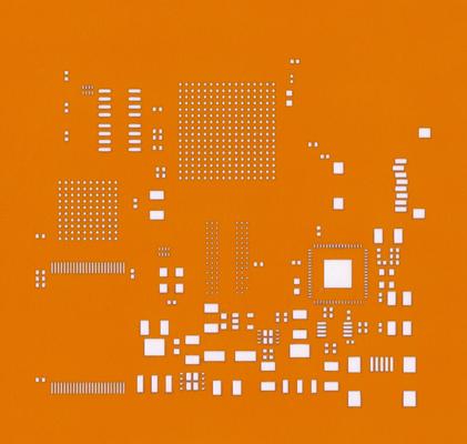
New Equipment | Solder Paste Stencils
For the DIYer, hobbyist or technical researcher there are times where all you need is a simple means to apply solder paste for SMT devices for a few simple boards. In those cases a plastic SMT stencil may be the right solution. Eliminate the tedious
Industry News | 2019-11-05 22:22:32.0
1. The definition of Sideplating Sideplating is actually the metalization of the board edge in PCB filed. Edge plating、Border plated、plated contour、side metal, these words can be used too to describe same function. 2. Sideplating Process Drilling - Milling plated Slots - Cleaning - Copper sink 3. Pictures to show the finished board’s sideplating
New Equipment | Test Equipment
Tebo-ICT is a kind of very professional ICT and ATE fixture software. Chinese interface, designed in humanity, compatible with Win98/2000/NT/XP/7/10 system, which is easy to operate and train. It can cope with all kinds of GERBER and buried via, posi
Technical Library | 2024-05-16 16:06:24.0
Much like actual cities where streets and roads connect buildings together, ICs on a board are connected to each other with copper traces. And just like any metropolitan city, urban expansion tends to move vertically instead of horizontally, but instead of multi-story buildings, we get multilayer boards. Vias are copper-plated holes spanning through the different layers of a given board or panel. They are the entrance locations to the subway stations, if you will. Having those multilayer boards has enabled electronic design to minimize the size of boards immensely without compromising on the complexity.

Definition: Drill pipe is hollow, thin-walled, steel or aluminium alloy piping used on drilling rigs. It is hollow to allow drilling fluid to be pumped down the hole through the bit and back up the annulus. Manufacturer process: Modern drill pi
Technical Library | 2024-04-29 21:39:52.0
In this paper, we develop and put into practice an Automatic Optical Inspection (AOI) system based on machine vision to check the holes on a printed circuit board (PCB). We incorporate the hardware and software. For the hardware part, we combine a PC, the three-axis positioning system, a lighting device and CCD cameras. For the software part, we utilize image registration, image segmentation, drill numbering, drill contrast, and defect displays to achieve this system. Results indicated that an accuracy of 5µm could be achieved in errors of the PCB holes allowing comparisons to be made. This is significant in inspecting the missing, the multi-hole and the incorrect location of the holes. However, previous work only focusses on one or other feature of the holes. Our research is able to assess multiple features: missing holes, incorrectly located holes and excessive holes. Equally, our results could be displayed as a bar chart and target plot. This has not been achieved before. These displays help users analyze the causes of errors and immediately correct the problems. Additionally, this AOI system is valuable for checking a large number of holes and finding out the defective ones on a PCB. Meanwhile, we apply a 0.1mm image resolution which is better than others used in industry. We set a detecting standard based on 2mm diameter of circles to diagnose the quality of the holes within 10 seconds.
Industry Directory | Manufacturer
Our company provides PCB's hole by using Mitsubishi CO2 laser drill machine.
Project Description | Parameters 12 Layer Thickness: 2.4+/-0.24 mm Min Hole Size: 0.25 mm Width/Space: 0.15mm/0.12 mm Surface Treatment: ENIG | Craft Black Drill 12 Layer | Application Consumer Electronics