ABSTRACT
This paper will review stencil design requirements for printing solder paste around and in through-hole pads / openings. There is much interest in this procedure since full implementation allows the placement of both through-hole components as well as SMD's and the subsequent reflow of both simultaneously. This in turn eliminates the need to wave solder or hand solder through-hole components.
Material type, pin type, lead length, and standoff height of the through hole components will be reviewed. Board design issues including plated through-hole size, pad size, board thickness, and solder mask type will also be reviewed. Three stencil designs will be considered: (1) Single thickness stencils with oversized stencil apertures for overprinting solder paste in the through hole pad areas; (2) Step stencils with oversized stencil apertures for overprinting solder paste in the through-hole pad areas; (3) Thick stencils (15mil to 25 mil thick) for printing solder paste in the through-hole pad areas. The latter thick stencil is the second stencil in the Two-Print stencil process.
The selection of stencil designs depends on several factors: Total solder volume requirement to fill the plated through- hole around the lead and form a proper solder fillet; Board thickness; Lead diameter; Plated through-hole size; Position of the through-hole component in the board layout; Pitch of the through-hole component; Surface energy of the solder mask, the activity level of the solder paste and the solderability of the metal to be soldered. Several examples will be reviewed with the recommended stencil designs.
BACKGROUND
Although the conversion from through-hole devices to SMT devices has been dramatic, several PCB's are still populated with both type of technology. In the majority of electronic assemblies there will be a few through-hole components remaining on the board. The connector, for example, in applications where robustness and/or power are required will continue to exist in through-hole configuration. There is great interest in placing and reflowing the through-hole components along with the SMT components. This presents specific challenges to the solder paste printing process. The stencil must provide enough solder paste volume to fill the hole and provide a good solder joint. The through-hole component must be able to withstand the extra heat encountered during the reflow process. Special considerations must be given to the through-hole lead configuration and the overall PCB design. Recent publications by Gervascio [1] and Whitmore et al [2] have explored the Pin-In-Paste process for through-hole reflow.
THROUGH-HOLE COMPONENT SELECTION
Component Material
Components often fall into the incompatible category because they are designed for wave soldering application, the wave soldering temperatures are typically 50oC to 100oC lower at the component body than the reflow process.
The following is a list of acceptable and unacceptable materials for reflow process:
Acceptable Materials: Diallyl Phthalate; FEP - Fluorinated Ethylene Propylene; Neoprene; Nylon 6/6; PFA - Perfluoroalkoxy Resin; Phenolic; Polyamide-imide; Polyarylsulfone; Polyester - Thermoset;
Polyetherimide; Polyethylene Terephthalate; Polyimide; Polysulfone; PFTE - Polytetrafluoroethylene;
Silicone; PPS - Polyphenylene Sulfide; LCP - Liquid Crystal Polymer; Polyetheretherketone.
Unacceptable materials: ABS - Acrylonitrile Butadiene Styrene; Acetal polymer; Acrylic; CAB - Cellulose Acetate Butyrate; PBT - Polybutylene Teraphthalate; Polybutylene; Polycarbonate; Polyethylene; Polyphenylene Oxide; Polypropylene; Polystyrene; PVC - Polyvinyl Chloride
PET - Polyethylene Tedrephthalate.
Pin type: Straight versus locking
Frequently through-hole components will have high retention forces, which are designed to maintain the components in place during wave solder process. In intrusive reflow these types of forces are not necessary to maintain the component in place. High insertion forces will complicate the manual or automation insertion and create opportunities for defects during the insertion or placement of the through-hole parts. The insertion force of the through-hole components must be less than the Z-axis force of the placement equipment, ideally the insertion force shall be approaching zero. The insertion shock must be kept to a minimum to prevent the dislodging of smaller SMT components. Components must be chosen with machine limitations (placement accuracy, placement force, vision capability, feeding mechanism) and ergonomic factors in mind. Through-hole components with a high pin count should have locating features for manual placement in order to guide the operators to the proper registration in pad holes.
Lead Length
The lead length should not exceed 0.050" greater than the PWB thickness. When the lead is inserted, some of the solder paste is pushed out of the hole and remains on the lead. If the lead is too long the solder paste will not flow back to the solder pad during the reflow process, reducing the final solder fillet volume.
PCB DESIGN ISSUES
Hole size
In analyzing the design of a component /hole size, several factors come into play. The hole size is a function of the following factors:
- Placement accuracy tolerance (A)
- PCB hole location tolerance (B)
- PCB hole size tolerance (C)
- Part lead location tolerance (D)
- Lead diameter tolerance (E)
Experience shows that the worst case analysis is not always necessary. Assuming that the above factors are normally and independently distributed and that the natural tolerance limits (+/-3 sigma) for each factor coincide with, or fall within, their respective specification limits, then taking the square root of the sum of the squares of the tolerances gives an estimate of the total standard deviation of the insertion process. The equation for determining component hole size is as follows:
Finished Hole diameter = Nominal lead diameter + (A2 +B2 + C2 + D2 + E2)1/2
The probability of successful insertion in the finished hole can be estimated from Z Tables, knowing that for a normal distribution the natural tolerance limits are
u +/- Za/2.s
However it should be noted that greater clearance between the component lead and the finished hole size will require more solder paste volume to form a proper solder joint.
Pad Size
When considering a minimum pad size the design must consider the finished hole size, PCB manufacturing tolerances and the minimum required annular ring. The minimum annular ring is the copper material measured from the edge of the hole to the outside diameter to the pad. This is a function of the minimum amount of layer-one copper needed to facilitate plating and mechanically anchor the plated through hole. The following will give the minimum land diameter for any finished hole size.
Minimum pad diameter = Finished hole diameter + 2x(minimum annular ring) + PCB manufacturing tolerances
It should be noted that a minimum pad size will reduce the solder paste volume required to form the top and bottom solder fillets.
Solder paste keep out area
The through hole components will require additional clearance around them that is free of components and non-masked vias, for solder paste overprint. If there are unmasked vias that are too close, solder will be shared between the via and component pad and a solder bridge can be formed. The solder paste keep out area around the through hole component should be clear of exposed metal, (other than the pad), other holes and legend ink. The legend ink might impact the flow of solder paste during reflow and cause it separate and form a solder bead.
Solder paste overprint consideration
Successful solder paste overprint is a function of the solder paste rheology, solder mask and through hole component stand off. Solder mask with a high surface energy will permit a larger overprint than a solder mask with a lower surface energy. In large overprint a solder bead can be formed with a low surface energy solder mask. In addition, more solderable land finish (e.g. HASL versus OSP), lead finish and a solder paste with higher wetting strength, all assist in making the overprint reflow process more robust. Solder paste print should cover the entire land, in order to maximize the wetting force exerted by the land on the overprinted areas.
The component stand off height required is a function of the solder paste volume extended beyond the component land. Since the shape of least energy for molten solder on an unsolderable surface is a sphere, there is a tendency for the overprinted paste to form into a spherical shape, as it moves inward toward the land during reflow. It can be seen that the component stand off must be > [ 2 x ((Solder volume printed beyond component land in any given direction x 3)/4P )1/3 ]. The component housing material should not come in contact with the solder paste. Where the stand off height cannot meet the above requirement, and the overprint pattern cannot be rearranged, it may be necessary to decrease the size of the overprint and make up the paste deficit by use of a stepped stencil.
Electrical test consideration
This process will impact the electrical in-circuit test. When the intrusive reflow process is used, the lead tip and the bottom solder fillet of the through-hole component is coated with flux residue and can cause an improper probe contact when the lead tip itself is being used as test site. An extra test pad will be required to eliminate the improper probe contact.
Another factor that might impact the electrical in-circuit test is the vacuum loss caused by the unplugged vias. For test purposes the non-test vias can be masked with solder mask.
STENCIL DESIGNS
Solder Volume
The objective of stencil printing of solder paste for the Through-Hole reflow process is to provide enough solder volume after reflow to fill the hole, create acceptable solder fillets aroung the leads. The equation describing the volume of solder paste required is shown in Figure 1. There are three stencil designs commonly used to deliver the through-hole solder paste: (1) Non-step stencil, (2) Step stencil, and (3) Two Print Stencil.
Minimum distance between aperture
The web distance between aperture shall be maximized in order to eliminate solder bridging and/or solder starvation caused by solder paste slumping. A thin web between aperture in stencil of 6 mil or less will distort and elongate during the printing process. Some of the following factors will affect the web dimension:
- Aperture size
- Stencil thickness
- Board flexure
- Squeegee material
- Printer set-up
Overprint w/o Step
This is a single thickness stencil with aperture sizes for the through-hole components oversized to meet the solder paste volume requirement to form a solder joint. A cross section of this type stencil is shown in Figure (2). An example of when this stencil could be used is a two row connector on 100 mil pitch with 45 mil diameter through-holes and 35 mil lead diameter with a 48 mil thick PCB and no other components and vias within 150 mil of the through-hole openings. An overprint stencil aperture of 85 mil wide and 170 mil long with a stencil thickness of 6 mil can deposit a sufficient solder paste volume to form a solder joint with solder fillets on both side of the PCB.
Overprint with Step
A step overprint stencil can be use when a single thickness overprint stencil will not provide a proper solder paste volume to form an acceptable solder joint. An application for the step overprint stencil is for a through-hole component with multiple lead rows (3 rows or more) or a dense populated board with a minimum keep-out area between the SMT components and the through-hole component. An example of this type stencil is shown in Figure 3. K1 and K2 are keep out distances. K2 is the distance between the through-hole aperture and the step 1 edge. As a design guide rule K2 can be as low as 25 mils. K1 is the distance from the step edge to the nearest aperture in the step-down area. As a design guide rule K1 should not be less than 35 mil for every mil of step-down thickness. For example an 8mil with a step down to 6 mil would require a K1 keep-out distance of 70 mils. It is also possible to put the step on the contact side of the stencil instead of the squeegee side, this is shown in Figure (4). This type of step is sometimes more convient when using metal squeegee blades. Contained solder paste heads do not have print blades ,as such, but they do have wiper blades. These wiper blades will catch on any step on the squeegee side of a stencil. Therefore contact side steps are required for this type of print head. The same keep-out rules apply for contact or squeegee side steps.
The layout of the step will depend on the layout of the PCB. Figure (5) shows a PCB with an edge connector. The PCB outline is indicated by the dotted line. In this case the step should be wider than the squeegee blade length as shown. The squeegee blade will not be held up on the ends as it passes into the step pocket for a squeeegee side step. The metal foil will easily deflect downward and make good gasketing contact to the PCB for the contact side step. Figure 6 shows through-hole components interwoven among SMT components. In this case the stencil is stepped down to 6 mil in a very large area that includes the board area. Again the step is larger than the squeegee blade length as shown. The stencil is stepped up to 8 mil in the area of the through-hole components. The step-up can be on the squeegee side or the contact side.
Two Print Stencil
Some through-hole devices have small leads with large holes or dense spacing with thick boards. In either case insufficient solder paste volume is available using the first two stencil designs. The Two Print stencil can deliver large amounts of solder paste volume into the plated through-holes. In this design a normal SMT stencil, typically 6 mils thick, is used to print the SMD solder bricks. While the SMD paste is still tacky a thick stencil is used to print the through-hole solder paste. Normally this requires a second stencil printer set up in line to perform this printing. This stencil can be as thick as required, however 16 to 30 mils is typical. When stencil thickness requirements exceed 20 mils, Laser-Cut Electropolished apertures provide better paste release and overall print performance due to the excellent wall geometry. The contact side of this stencil is relief etched at least 10 mils deep in any area where SMD bricks have been previously printed. A cross section of the Two Print Through-Hole Stencil is shown in Figure (7).
CONCLUSION
Many SMT assembly process engineers have been successful in converting Through-Hole assembly from a wave soldering process to a reflow process. This allows both types of components to be placed on or into the PCB and soldered in place with a single reflow process. There are a number of design issues to consider when converting to this process as well as a myriad of trade-off's. However careful selection of the Through-Hole component material type, Pin design, Lead length, PCB design, and Stencil design will assure success.
REFERENCES:
[1] T. Gervascio, "Developing the Paste-In-Hole Process, Proceedings of Surface Mount International" 1994, p.333
[2] D.Manessia, M. Whitmore, J.H.Adriance, and G.R. Westby, "Evaluation Study of Proflow System for Stencil Printing of Thick Boards (.125") in the Alternative Assembly and Reflow Technologh (AART) or Pin-In-Paste Process", Proceedings of the Technical Program NEPCON West 99, p.416
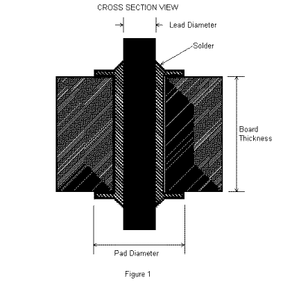
Figure 1
Vsp = (((Vpth + 2 x Vfillet ��� Vlead) / % metal content of solder paste by volume) x % paste release from stencil) ��� Vphole
Where the % paste release from the stencil may be greater than 100% for an off contact print.
Vsp Volume of solder paste required
Vpth Volume of plated through-hole (P x radius of plated through-hole2) x board thickness
Vlead Volume of lead:
- a) round lead = (P x radius of component lead2) x (board thickness + (2 x fillet height)
- b) square lead = (length lead x width lead) x (board thickness + ( 2 x fillets height))
- Where fillet height = (diameter of solder pad ��� lead diameter)/2
Vfillet Volume of the solder fillets
- The solder fillet volume is calculated by employing the Papus rule which states: The volume of solid body
- formed by revolution equals the area of the surface multiplied by the length of the path of its center of gravity.
- Volume fillet = 0.215r2 x (0.2234r + (lead diameter/2)) x 2P
- Where r = (Diameter of solder pad ��� lead diameter)/2
Vphole Volume of solder in the plated hole. This volume will be dependent of the hole size and your printing process.

Figure 2

Figure 3

Figure 4

Figure 5
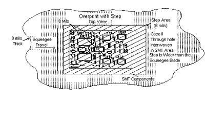
Figure 6

Figure 7