 Aug 02, 2017
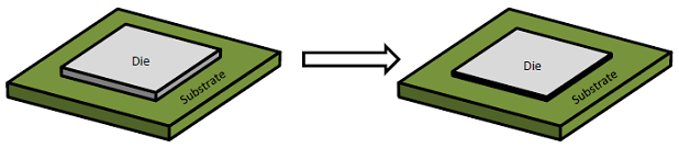

As market leader in bond testing, XYZTEC is pushing the technology forward. In this month's newsletter we highlight the recent advances in thin, 3D and MEMS die bond testing. As developments in thin die change the shape of our customers' products, three fundamental difficulties for the bond test have to be overcome:
The reduced ratio of die thickness to die bond area
The first difficulty is the reduction in test load area to bond area as the die becomes thinner. This is especially problematic when shear testing, because there is less area to apply the test load to. As the die thickness reduces there comes a point when the test load stress between the tool and the die reaches its yield value before the bond reaches its yield stress. The die then fails before the bond and the bond strength is not measured.
Warped die and substrate increases buckling loads on die that can cause it to fracture before the bond fails
The second difficulty relates to both shear and stud pull testing, namely the fact that die and substrate warpage with thin die are likely to occur. When shear testing, warped die and substrate increase buckling loads on the die that can cause it to fracture before the bond fails. For stud pull, warpage makes a strong and consistent glue layer thickness between the stud and die difficult.
Thirdly, when silicon is directly bonded to silicon or other similar materials the bond strength is very high. This makes testing exceptionally difficult, both when performing shear and stud pull.
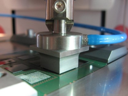
Maximum recorded stress on the die edge up to 1200MPa
45° Self aligning top landing tool
To obtain the failure mode of interest i.e. a bond failure, we must be able to load the bond to the highest force possible. XYZTEC has achieved positive results by combining several techniques to significantly increase the maximum loads possible. The picture shows our patented 45° self aligning top landing tool.
Flip chip and soldered die applications have been successfully sheared, applying up to 1200MPa on the side edge of die.


