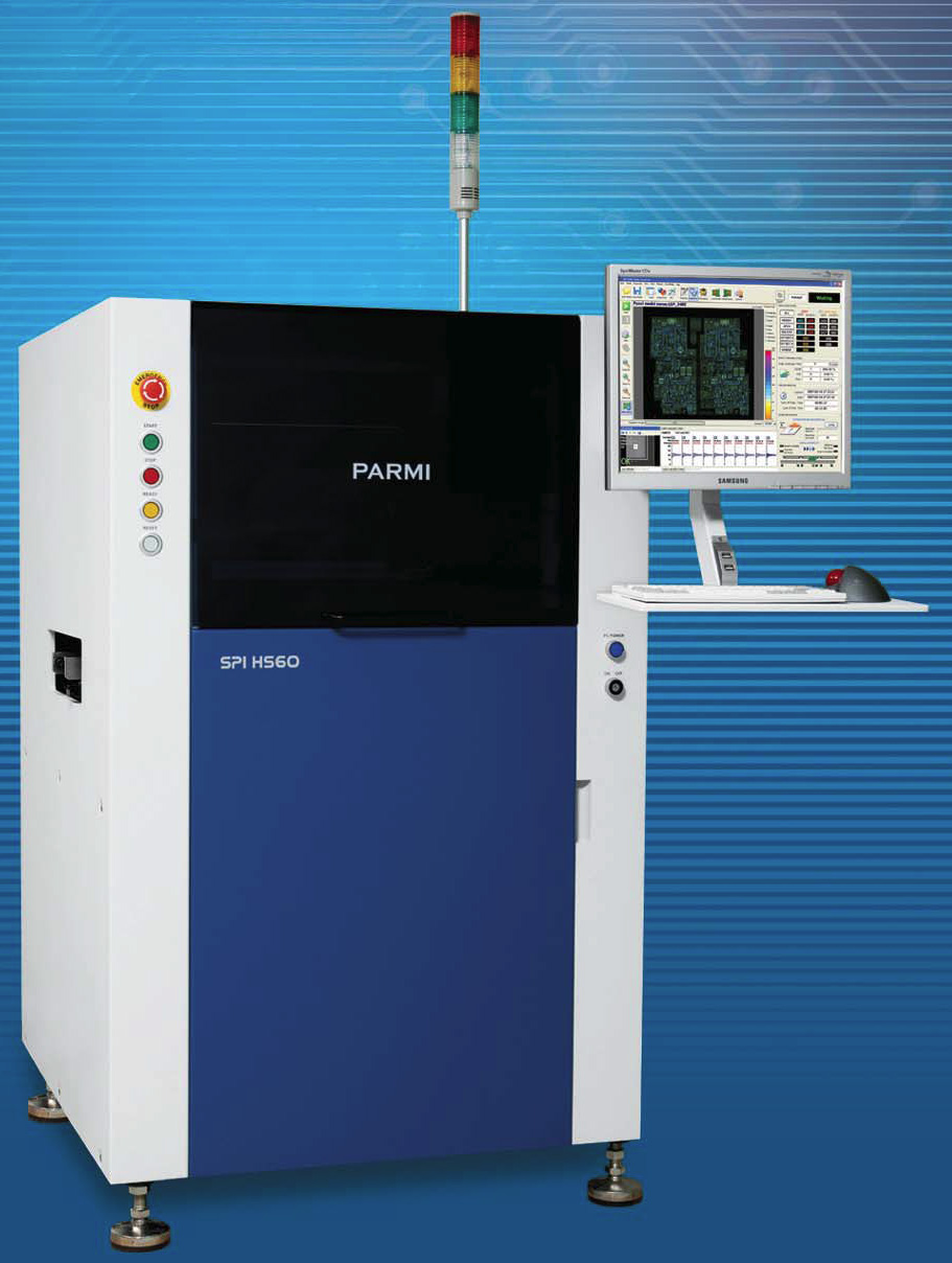
SPI HS60 - 3D Solder Paste Inspection System
Company Information:
Name: |
SPI HS60 - 3D Solder Paste Inspection System |
Category: |
|
Offered by: |
|
SPI HS60 - 3D Solder Paste Inspection System Description:
The most reliable and accurate 3D data
Our innovative 3D laser triangulation sensor, RSC profiles exactly real shape of features and also provides very robust 3D data against considerable variations of PCB color and finishing condition, solder material, paste shape, and warpage.
This highest quality of 3D data backs up top level performance of SPI HS60 system concerning about the reliability and accuracy. And It’s due to PARMI’s unique signal processing technology that is implemented as hardware logic.
The utmost inspection speed
By virtue of affordable profiles speed of the 3D sensor, the SPI HS60 system provides 100% whole pads inspection in even fast assemble lines.
The lateral resolution is set at 18 ㎛ along the X axis direction and the scan resolution along the Y axis is set at 20㎛ . This provides the system enables to inspect an area of 60㎠ per second. This utmost inspection speed with best quality 3D data differentiates the SPI HS60 system from other systems and leads the SPI HS60 system to the top level.
Authentic Inspection and measurement with no false call
Our intelligent vision algorithm backed by high quality 3D data detects every kind of defected pads. The measurable items are height, area, volume, and positional offset pads that deviate from tolerance limits. And also the algorithm detects bridged pads in a very reliable manner.
The considerable design concepts such as rotated laser sheet beam against the scan direction and small angle between laser sheet beam and camera optical axis for negligible shadow effect secure much better performance for repeatability and accuracy.
Even for small CSPs and fine pitch QFPs, Gage R&R are much less than 10% for both height and volume data.
Fast job change and easy operation
The job change consists of two stages. First stage is making a teaching file. Teaching process done by using Gerberworks takes normally less than a half hour even in the case of complex PCBs. The Gerberworks inputs industry standard RS-274X format file and prepare a hierarchy of information on a pad, component, and array board level, that are used during PCB inspection. For the component level measurement and analysis, some CAD and BOM files can be imported. Teaching process using Gerberworkscan be done on-line or off-line. And machine setting that is second stage, such as tolerance setting, only requires 10 minutes. This extremely short job change time save customer’s valuable time.
The user interface of inspection program SPIworks is based on voice of able field engineers, therefore it features intuition and easiness to field engineers. And the UI also provides diverse useful functions for printing process monitoring and analysis.
X-bar and X charts
- X-bar & Variance chart
- Measured data list
- 3D Shape viewer
- Defect Image List
- Offset graph
Clear and prompt insight into printing process
Not only to detect defect, but also to help customer to control printing process by giving data and guide line is another very important role. Besides the independent SPC program SPCworks, SPIworks embeds very intuitive SPC functions for field operator’s prompt treatment on screen printer.
Coloring amplitude of measured data, sigma values, and defect frequencies on every pad in the main viewer gives operators get prompt insight into printing process. And also the X-bar & variance chart let operator monitor and understand entire printing process with ease. Operator’s correct treatment could prevent defect and secure quality of printing process. We know that it is PARMI’s unique and elegant attitude to move one more step toward valuable and useful machine for customers.
Defect confirmation and review
The detected defects are possible to be identified by Defect List Viewer such as details of defect panels, measured data of defect pads, 2D and 3D images of defect pastes. Moreover, defect analysis work can be easily done by configuring defect analysis conditions to list only wanted defect items.
SPI HS60 - 3D Solder Paste Inspection System was added in Feb 2013
SPI HS60 - 3D Solder Paste Inspection System has been viewed 1734 times
2 More Products from PARMI :